- 您现在的位置:买卖IC网 > PDF目录358105 > M24C16-WMB6 (意法半导体) The CAT24FC02 is a 2-kb Serial CMOS EEPROM internally organized as 256 words of 8 bits each PDF资料下载
参数资料
| 型号: | M24C16-WMB6 |
| 厂商: | 意法半导体 |
| 元件分类: | DRAM |
| 英文描述: | The CAT24FC02 is a 2-kb Serial CMOS EEPROM internally organized as 256 words of 8 bits each |
| 中文描述: | 该CAT24FC02是一个2 KB的EEPROM的国内256个8位每字举办的串行CMOS |
| 文件页数: | 6/25页 |
| 文件大小: | 449K |
| 代理商: | M24C16-WMB6 |
M24C16, M24C08, M24C04, M24C02, M24C01
6/25
DEVICE OPERATION
The device supports the I2C protocol. This is sum-
marized in
Figure 6.
. Any device that sends data
on to the bus is defined to be a transmitter, and
any device that reads the data to be a receiver.
The device that controls the data transfer is known
as the bus master, and the other as the slave de-
vice. A data transfer can only be initiated by the
bus master, which will also provide the serial clock
for synchronization. The M24Cxx device is always
a slave in all communication.
Start Condition
Start is identified by a falling edge of Serial Data
(SDA) while Serial Clock (SCL) is stable in the
High state. A Start condition must precede any
data transfer command. The device continuously
monitors (except during a Write cycle) Serial Data
(SDA) and Serial Clock (SCL) for a Start condition,
and will not respond unless one is given.
Stop Condition
Stop is identified by a rising edge of Serial Data
(SDA) while Serial Clock (SCL) is stable and driv-
en High. A Stop condition terminates communica-
tion between the device and the bus master. A
Read command that is followed by NoAck can be
followed by a Stop condition to force the device
into the Stand-by mode. A Stop condition at the
end of a Write command triggers the internal Write
cycle.
Acknowledge Bit (ACK)
The acknowledge bit is used to indicate a success-
ful byte transfer. The bus transmitter, whether it be
bus master or slave device, releases Serial Data
(SDA) after sending eight bits of data. During the
9
th
clock pulse period, the receiver pulls Serial
Data (SDA) Low to acknowledge the receipt of the
eight data bits.
Data Input
During data input, the device samples Serial Data
(SDA) on the rising edge of Serial Clock (SCL).
For correct device operation, Serial Data (SDA)
must be stable during the rising edge of Serial
Clock (SCL), and the Serial Data (SDA) signal
must change
only
when Serial Clock (SCL) is driv-
en Low.
Memory Addressing
To start communication between the bus master
and the slave device, the bus master must initiate
a Start condition. Following this, the bus master
sends the Device Select Code, shown in
Table 3.
(on Serial Data (SDA), most significant bit first).
The Device Select Code consists of a 4-bit Device
Type Identifier, and a 3-bit Chip Enable “Address”
(E2, E1, E0). To address the memory array, the 4-
bit Device Type Identifier is 1010b.
Each device is given a unique 3-bit code on the
Chip Enable (E0, E1, E2) inputs. When the Device
Select Code is received, the device only responds
if the Chip Enable Address is the same as the val-
ue on the Chip Enable (E0, E1, E2) inputs. How-
ever, those devices with larger memory capacities
(the M24C16, M24C08 and M24C04) need more
address bits. E0 is not available for use on devices
that need to use address line A8; E1 is not avail-
able for devices that need to use address line A9,
and E2 is not available for devices that need to use
address line A10 (see
Figure 3.
and
Table 3.
for
details). Using the E0, E1 and E2 inputs, up to
eight M24C02 (or M24C01), four M24C04, two
M24C08 or one M24C16 devices can be connect-
ed to one I2C bus. In each case, and in the hybrid
cases, this gives a total memory capacity of
16 Kbits, 2 KBytes (except where M24C01 devic-
es are used).
The 8
th
bit is the Read/Write bit (RW). This bit is
set to 1 for Read and 0 for Write operations.
If a match occurs on the Device Select code, the
corresponding device gives an acknowledgment
on Serial Data (SDA) during the 9
th
bit time. If the
device does not match the Device Select code, it
deselects itself from the bus, and goes into Stand-
by mode.
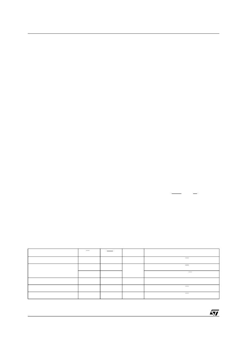
Table 4. Operating Modes
Note: 1. X =
V
IH
or V
IL
.
Mode
RW bit
WC
1
Bytes
Initial Sequence
Current Address Read
1
X
1
START, Device Select, RW = 1
Random Address Read
0
X
1
START, Device Select, RW = 0, Address
1
X
reSTART, Device Select, RW = 1
Sequential Read
1
X
≥
1
Similar to Current or Random Address Read
Byte Write
0
V
IL
1
START, Device Select, RW = 0
Page Write
0
V
IL
≤
16
START, Device Select, RW = 0
相关PDF资料 |
PDF描述 |
|---|---|
| M24C16-WMB6G | The CAT24FC02 is a 2-kb Serial CMOS EEPROM internally organized as 256 words of 8 bits each |
| M24C16-WMB6P | The CAT24FC02 is a 2-kb Serial CMOS EEPROM internally organized as 256 words of 8 bits each |
| M24C16-WMB6T | The CAT24FC02 is a 2-kb Serial CMOS EEPROM internally organized as 256 words of 8 bits each |
| M24C16-WMB6TG | The CAT24FC02 is a 2-kb Serial CMOS EEPROM internally organized as 256 words of 8 bits each |
| M24C16-WMB6TP | The CAT24FC02 is a 2-kb Serial CMOS EEPROM internally organized as 256 words of 8 bits each |
相关代理商/技术参数 |
参数描述 |
|---|---|
| M24C16-WMB6TG | 功能描述:电可擦除可编程只读存储器 2.5-5.5V 16K (2Kx8) RoHS:否 制造商:Atmel 存储容量:2 Kbit 组织:256 B x 8 数据保留:100 yr 最大时钟频率:1000 KHz 最大工作电流:6 uA 工作电源电压:1.7 V to 5.5 V 最大工作温度:+ 85 C 安装风格:SMD/SMT 封装 / 箱体:SOIC-8 |
| M24C16-WMN6 | 功能描述:电可擦除可编程只读存储器 5.5V 16K (2Kx8) RoHS:否 制造商:Atmel 存储容量:2 Kbit 组织:256 B x 8 数据保留:100 yr 最大时钟频率:1000 KHz 最大工作电流:6 uA 工作电源电压:1.7 V to 5.5 V 最大工作温度:+ 85 C 安装风格:SMD/SMT 封装 / 箱体:SOIC-8 |
| M24C16-WMN6G | 功能描述:电可擦除可编程只读存储器 2.5-5.5V 16K (2Kx8) RoHS:否 制造商:Atmel 存储容量:2 Kbit 组织:256 B x 8 数据保留:100 yr 最大时钟频率:1000 KHz 最大工作电流:6 uA 工作电源电压:1.7 V to 5.5 V 最大工作温度:+ 85 C 安装风格:SMD/SMT 封装 / 箱体:SOIC-8 |
| M24C16WMN6P | 制造商:STMicroelectronics 功能描述: |
| M24C16-WMN6P | 功能描述:电可擦除可编程只读存储器 2.5-5.5V 16K (2Kx8) RoHS:否 制造商:Atmel 存储容量:2 Kbit 组织:256 B x 8 数据保留:100 yr 最大时钟频率:1000 KHz 最大工作电流:6 uA 工作电源电压:1.7 V to 5.5 V 最大工作温度:+ 85 C 安装风格:SMD/SMT 封装 / 箱体:SOIC-8 |
发布紧急采购,3分钟左右您将得到回复。