- 您现在的位置:买卖IC网 > PDF目录358977 > M27C1001-10XN1TR (意法半导体) 1 Mbit 128Kb x8 UV EPROM and OTP EPROM PDF资料下载
参数资料
| 型号: | M27C1001-10XN1TR |
| 厂商: | 意法半导体 |
| 英文描述: | 1 Mbit 128Kb x8 UV EPROM and OTP EPROM |
| 中文描述: | 1兆位存储器的128KB x8紫外线和OTP存储器 |
| 文件页数: | 5/17页 |
| 文件大小: | 159K |
| 代理商: | M27C1001-10XN1TR |
5/17
M27C1001
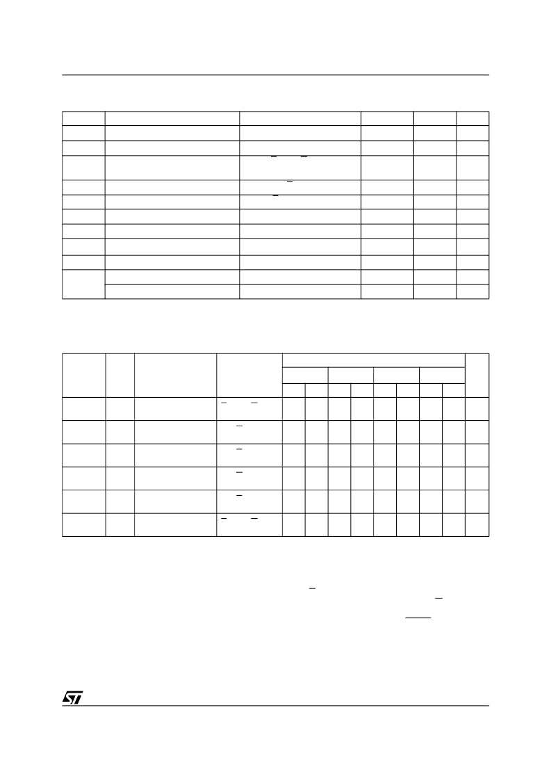
Table 7. Read Mode DC Characteristics
(1)
(TA = 0 to 70°C, –40 to 85°C or –40 to 125°C; V
CC
= 5V ± 5% or 5V ± 10%; V
PP
= V
CC
)
Symbol
Parameter
Note: 1. V
CC
must be applied simultaneously with or before V
PP
and removed simultaneously or after V
PP
.
2. Maximum DC voltage on Output is V
CC
+0.5V.
Table 8A. Read Mode AC Characteristics
(1)
(TA = 0 to 70°C, –40 to 85°C or –40 to 125°C; V
CC
= 5V ± 5% or 5V ± 10%; V
PP
= V
CC
)
Note: 1. V
CC
must be applied simultaneously with or before V
PP
and removed simultaneously or after V
PP
.
2. Sampled only, not 100% tested.
3. Speed obtained with High Speed AC measurement conditions.
Test Condition
Min
Max
Unit
I
LI
Input Leakage Current
0V
≤
V
IN
≤
V
CC
0V
≤
V
OUT
≤
V
CC
±10
μA
I
LO
Output Leakage Current
±10
μA
I
CC
Supply Current
E = V
IL
, G = V
IL
,
I
OUT
= 0mA, f = 5MHz
30
mA
I
CC1
Supply Current (Standby) TTL
E = V
IH
1
mA
I
CC2
Supply Current (Standby) CMOS
E > V
CC
– 0.2V
100
μA
I
PP
Program Current
V
PP
= V
CC
10
μA
V
IL
Input Low Voltage
–0.3
0.8
V
V
IH
(2)
Input High Voltage
2
V
CC
+ 1
V
V
OL
Output Low Voltage
I
OL
= 2.1mA
0.4
V
V
OH
Output High Voltage TTL
I
OH
= –400μA
2.4
V
Output High Voltage CMOS
I
OH
= –100μA
V
CC
– 0.7V
V
Symbol
Alt
Parameter
Test Condition
M27C1001
Unit
-35
(3)
-45
-60
-70
Min
Max
Min
Max
Min
Max
Min
Max
t
AVQV
t
ACC
Address Valid to
Output Valid
E = V
IL
, G = V
IL
35
45
60
70
ns
t
ELQV
t
CE
Chip Enable Low to
Output Valid
G = V
IL
35
45
60
70
ns
t
GLQV
t
OE
Output Enable Low
to Output Valid
E = V
IL
25
25
30
35
ns
t
EHQZ
(2)
t
DF
Chip Enable High to
Output Hi-Z
G = V
IL
0
25
0
25
0
30
0
30
ns
t
GHQZ (2)
t
DF
Output Enable High
to Output Hi-Z
E = V
IL
0
25
0
25
0
30
0
30
ns
t
AXQX
t
OH
Address Transition
to Output Transition
E = V
IL
, G = V
IL
0
0
0
0
ns
Two Line Output Control
Because EPROMs are usually used in larger
memory arrays, this product features a 2 line con-
trol function which accommodates the use of mul-
tiple memory connection. The two line control
function allows:
a. the lowest possible memory power dissipation,
b. complete assurance that output bus contention
will not occur.
For the most efficient use of these two control
lines, E should be decoded and used as the prima-
ry device selecting function, while G should be
made a common connection to all devices in the
array and connected to the READ line from the
system control bus. This ensures that all deselect-
ed memory devices are in their low power standby
mode and that the output pins are only active
when data is required from a particular memory
device.
相关PDF资料 |
PDF描述 |
|---|---|
| M27C1001-90XN1TR | 1 Mbit 128Kb x8 UV EPROM and OTP EPROM |
| M27C1001-80XN1TR | 1 Mbit 128Kb x8 UV EPROM and OTP EPROM |
| M27C1001-70XN1TR | 1 Mbit 128Kb x8 UV EPROM and OTP EPROM |
| M27C1001-60XN1TR | 1 Mbit 128Kb x8 UV EPROM and OTP EPROM |
| M27C1001-25XN1X | 1 Mbit 128Kb x8 UV EPROM and OTP EPROM |
相关代理商/技术参数 |
参数描述 |
|---|---|
| M27C1001-10XN1X | 制造商:STMICROELECTRONICS 制造商全称:STMicroelectronics 功能描述:1 Mbit 128Kb x8 UV EPROM and OTP EPROM |
| M27C1001-10XN3TR | 制造商:STMICROELECTRONICS 制造商全称:STMicroelectronics 功能描述:1 Mbit 128Kb x8 UV EPROM and OTP EPROM |
| M27C1001-10XN3X | 制造商:STMICROELECTRONICS 制造商全称:STMicroelectronics 功能描述:1 Mbit 128Kb x8 UV EPROM and OTP EPROM |
| M27C1001-10XN6TR | 制造商:STMICROELECTRONICS 制造商全称:STMicroelectronics 功能描述:1 Mbit 128Kb x8 UV EPROM and OTP EPROM |
| M27C1001-10XN6X | 制造商:STMICROELECTRONICS 制造商全称:STMicroelectronics 功能描述:1 Mbit 128Kb x8 UV EPROM and OTP EPROM |
发布紧急采购,3分钟左右您将得到回复。