- 您现在的位置:买卖IC网 > PDF目录358977 > M27C1001-10XN1TR (意法半导体) 1 Mbit 128Kb x8 UV EPROM and OTP EPROM PDF资料下载
参数资料
| 型号: | M27C1001-10XN1TR |
| 厂商: | 意法半导体 |
| 英文描述: | 1 Mbit 128Kb x8 UV EPROM and OTP EPROM |
| 中文描述: | 1兆位存储器的128KB x8紫外线和OTP存储器 |
| 文件页数: | 6/17页 |
| 文件大小: | 159K |
| 代理商: | M27C1001-10XN1TR |
M27C1001
6/17
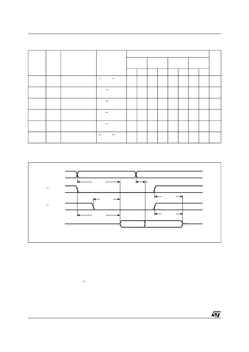
Figure 5. Read Mode AC Waveforms
AI00713B
tAXQX
tEHQZ
A0-A16
E
G
Q0-Q7
tAVQV
tGHQZ
tGLQV
tELQV
VALID
Hi-Z
VALID
Table 8B. Read Mode AC Characteristics
(1)
(TA = 0 to 70°C, –40 to 85°C or –40 to 125°C; V
CC
= 5V ± 5% or 5V ± 10%; V
PP
= V
CC
)
Note: 1. V
CC
must be applied simultaneously with or before V
PP
and removed simultaneously or after V
PP
.
2. Sampled only, not 100% tested.
Symbol
Alt
Parameter
Test Condition
M27C1001
Unit
-80
-90
-10
-12/-15/
-20/-25
Min
Max
Min
Max
Min
Max
Min
Max
t
AVQV
t
ACC
Address Valid to
Output Valid
E = V
IL
, G = V
IL
80
90
100
120
ns
t
ELQV
t
CE
Chip Enable Low to
Output Valid
G = V
IL
80
90
100
120
ns
t
GLQV
t
OE
Output Enable Low
to Output Valid
E = V
IL
40
45
50
60
ns
t
EHQZ (2)
t
DF
Chip Enable High to
Output Hi-Z
G = V
IL
0
30
0
30
0
30
0
40
ns
t
GHQZ (2)
t
DF
Output Enable High
to Output Hi-Z
E = V
IL
0
30
0
30
0
30
0
40
ns
t
AXQX
t
OH
Address Transition
to Output Transition
E = V
IL
, G = V
IL
0
0
0
0
ns
System Considerations
The power switching characteristics of Advanced
CMOS EPROMs require careful decoupling of the
devices. The supply current, I
CC
, has three seg-
ments that are of interest to the system designer:
the standby current level, the active current level,
and transient current peaks that are produced by
the falling and rising edges of E. The magnitude of
the transient current peaks is dependent on the
capacitive and inductive loading of the device at
the output. The associated transient voltage peaks
can be suppressed by complying with the two line
output control and by properly selected decoupling
capacitors. It is recommended that a 0.1μF ceram-
ic capacitor be used on every device between V
CC
and V
SS
. This should be a high frequency capaci-
tor of low inherent inductance and should be
placed as close to the device as possible. In addi-
tion, a 4.7μF bulk electrolytic capacitor should be
used between V
CC
and V
SS
for every eight devic-
es. The bulk capacitor should be located near the
power supply connection point. The purpose of the
bulk capacitor is to overcome the voltage drop
caused by the inductive effects of PCB traces.
相关PDF资料 |
PDF描述 |
|---|---|
| M27C1001-90XN1TR | 1 Mbit 128Kb x8 UV EPROM and OTP EPROM |
| M27C1001-80XN1TR | 1 Mbit 128Kb x8 UV EPROM and OTP EPROM |
| M27C1001-70XN1TR | 1 Mbit 128Kb x8 UV EPROM and OTP EPROM |
| M27C1001-60XN1TR | 1 Mbit 128Kb x8 UV EPROM and OTP EPROM |
| M27C1001-25XN1X | 1 Mbit 128Kb x8 UV EPROM and OTP EPROM |
相关代理商/技术参数 |
参数描述 |
|---|---|
| M27C1001-10XN1X | 制造商:STMICROELECTRONICS 制造商全称:STMicroelectronics 功能描述:1 Mbit 128Kb x8 UV EPROM and OTP EPROM |
| M27C1001-10XN3TR | 制造商:STMICROELECTRONICS 制造商全称:STMicroelectronics 功能描述:1 Mbit 128Kb x8 UV EPROM and OTP EPROM |
| M27C1001-10XN3X | 制造商:STMICROELECTRONICS 制造商全称:STMicroelectronics 功能描述:1 Mbit 128Kb x8 UV EPROM and OTP EPROM |
| M27C1001-10XN6TR | 制造商:STMICROELECTRONICS 制造商全称:STMicroelectronics 功能描述:1 Mbit 128Kb x8 UV EPROM and OTP EPROM |
| M27C1001-10XN6X | 制造商:STMICROELECTRONICS 制造商全称:STMicroelectronics 功能描述:1 Mbit 128Kb x8 UV EPROM and OTP EPROM |
发布紧急采购,3分钟左右您将得到回复。