- 您现在的位置:买卖IC网 > PDF目录365220 > M38748EAF-XXXFS (Mitsubishi Electric Corporation) SINGLE-CHIP 8-BIT CMOS MICROCOMPUTER PDF资料下载
参数资料
| 型号: | M38748EAF-XXXFS |
| 厂商: | Mitsubishi Electric Corporation |
| 英文描述: | SINGLE-CHIP 8-BIT CMOS MICROCOMPUTER |
| 中文描述: | 单芯片8位CMOS微机 |
| 文件页数: | 46/92页 |
| 文件大小: | 1292K |
| 代理商: | M38748EAF-XXXFS |
第1页第2页第3页第4页第5页第6页第7页第8页第9页第10页第11页第12页第13页第14页第15页第16页第17页第18页第19页第20页第21页第22页第23页第24页第25页第26页第27页第28页第29页第30页第31页第32页第33页第34页第35页第36页第37页第38页第39页第40页第41页第42页第43页第44页第45页当前第46页第47页第48页第49页第50页第51页第52页第53页第54页第55页第56页第57页第58页第59页第60页第61页第62页第63页第64页第65页第66页第67页第68页第69页第70页第71页第72页第73页第74页第75页第76页第77页第78页第79页第80页第81页第82页第83页第84页第85页第86页第87页第88页第89页第90页第91页第92页
46
3874 Group
SINGLE-CHIP 8-BIT CMOS MICROCOMPUTER
MITSUBISHI MICROCOMPUTERS
G
S
BUSY3
input signal
The S
BUSY3
input is a signal which receives a request for a stop of
transmission/reception from the serial transfer destination.
When the internal synchronous clock is selected, input an “H” level
signal into the S
BUSY3
input and an “L” level signal into the S
BUSY3
input in the initial status in which transfer is stopped.
When starting a transmit/receive operation, input an “L” level signal
into the S
BUSY3
input and an “H” level signal into the S
BUSY3
input
in the period of 1.5 cycles or more of the transfer clock. Then,
transfer clocks are output from the S
CLK3
output.
When an “H” level signal is input into the S
BUSY3
input and an “L”
level signal into the S
BUSY3
input after a transmit/receive operation
is started, this transmit/receive operation are not stopped immedi-
ately and the transfer clocks from the S
CLK3
output are not
stopped until the specified number of bits is transmitted and re-
ceived.
The handshake unit of the 8-bit serial I/O is 8 bits and that of the
arbitrary bit serial I/O is the bit number adding “1” to the set value
to the transfer counter, and that of the automatic transfer serial I/O
is 8 bits.
Handshake Signal
G
S
STB3
output signal
The S
STB3
output is a signal to inform an end of transmission/re-
ception to the serial transfer destination . The S
STB3
output signal
can be used only when the internal synchronous clock is selected.
In the initial status, that is, in the status in which the serial I/O ini-
tialization bit (b4) is reset to “0”, the S
STB3
output goes to “L”, and
the S
STB3
output goes to “H”.
At the end of transmit/receive operation, when the data of the se-
rial I/O3 register is all output from S
OUT3
, pulses which are the
S
STB3
output of “H” and the S
STB3
output of “L” are output in the
period of 1 cycle of the transfer clock. After that, each pulse is re-
turned to the initial status in which S
STB3
output goes to “L” and
the S
STB3
output goes to “H”.
Furthermore, after 1 cycle, the serial transfer status flag (b5) is re-
set to “0”.
In the automatic transfer serial I/O mode, whether making the
S
STB3
output active at an end of each 1-byte data or after comple-
tion of transfer of all data can be selected by the S
BUSY3
output
S
STB3
output function selection bit (b4 of address 0015
16
) of serial
I/O3 control register 2.
When the external synchronous clock is selected, input an “H”
level signal into the S
BUSY3
input and an “L” level signal into the
S
BUSY3
input in the initial status in which transfer is stopped. At
this time, the transfer clocks to be input in S
CLK3
become invalid.
During serial transfer, the transfer clocks to be input in S
CLK3
be-
come valid, enabling a transmit/receive operation, while an “L”
level signal is input into the S
BUSY3
input and an “H” level signal is
input into the S
BUSY3
input.
When changing the input values in to the S
BUSY3
input and the
S
BUSY3
input in these operations, change them while the S
CLK3
in-
put is in a high state.
When the high impedance of the S
OUT3
output is selected by the
S
OUT3
output control bit (b6), the S
OUT3
output becomes active,
enabling serial transfer by inputting a transfer clock to S
CLK3
, while
an “L” level signal is input into the S
BUSY3
input and an “H” level
signal is input into the S
BUSY3
input.
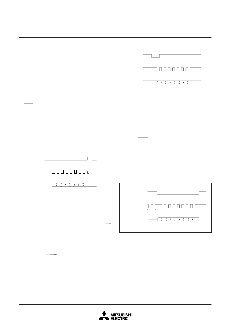
Fig. 40 S
STB3
output operation
Fig. 41 S
BUSY3
input operation (internal synchronous clock)
G
S
BUSY3
output signal
The S
BUSY3
output is a signal which requests a stop of transmis-
sion/reception to the serial transfer destination. In the automatic
transfer serial I/O mode, regardless of the internal or external syn-
chronous clock, whether making the S
BUSY3
output active at
transfer of each 1-byte data or during transfer of all data can be
selected by the S
BUSY3
output S
STB3
output function selection bit
(b4).
In the initial status, that is, the status in which the serial I/O initial-
ization bit (b4) is reset to “0”, the S
BUSY3
output goes to “H” and
the S
BUSY3
output goes to “L”.
Fig. 42 S
BUSY3
input operation (external synchronous clock)
S
STB3
S
CLK3
S
OUT3
S
BUSY3
S
CLK3
S
OUT3
S
BUSY3
S
CLK3
S
OUT3
Invalid
(Output high-impedance)
相关PDF资料 |
PDF描述 |
|---|---|
| M38748EAF-XXXGP | SINGLE-CHIP 8-BIT CMOS MICROCOMPUTER |
| M38748EDD-XXXFS | SINGLE-CHIP 8-BIT CMOS MICROCOMPUTER |
| M38748EDD-XXXGP | SINGLE-CHIP 8-BIT CMOS MICROCOMPUTER |
| M38748EDF-XXXFS | SINGLE-CHIP 8-BIT CMOS MICROCOMPUTER |
| M38748EDF-XXXGP | SINGLE-CHIP 8-BIT CMOS MICROCOMPUTER |
相关代理商/技术参数 |
参数描述 |
|---|---|
| M38748EAF-XXXGP | 制造商:MITSUBISHI 制造商全称:Mitsubishi Electric Semiconductor 功能描述:SINGLE-CHIP 8-BIT CMOS MICROCOMPUTER |
| M38748EAT-XXXFS | 制造商:MITSUBISHI 制造商全称:Mitsubishi Electric Semiconductor 功能描述:SINGLE-CHIP 8-BIT CMOS MICROCOMPUTER |
| M38748EAT-XXXGP | 制造商:MITSUBISHI 制造商全称:Mitsubishi Electric Semiconductor 功能描述:SINGLE-CHIP 8-BIT CMOS MICROCOMPUTER |
| M38748EBD-XXXFS | 制造商:MITSUBISHI 制造商全称:Mitsubishi Electric Semiconductor 功能描述:SINGLE-CHIP 8-BIT CMOS MICROCOMPUTER |
| M38748EBD-XXXGP | 制造商:MITSUBISHI 制造商全称:Mitsubishi Electric Semiconductor 功能描述:SINGLE-CHIP 8-BIT CMOS MICROCOMPUTER |
发布紧急采购,3分钟左右您将得到回复。