- 您现在的位置:买卖IC网 > PDF目录80583 > M38D59GF-XXXFP 8-BIT, MROM, 6.25 MHz, MICROCONTROLLER, PQFP80 PDF资料下载
参数资料
| 型号: | M38D59GF-XXXFP |
| 元件分类: | 微控制器/微处理器 |
| 英文描述: | 8-BIT, MROM, 6.25 MHz, MICROCONTROLLER, PQFP80 |
| 封装: | 14 X 20 MM, 0.80 MM PITCH, PLASTIC, QFP-80 |
| 文件页数: | 63/142页 |
| 文件大小: | 2004K |
| 代理商: | M38D59GF-XXXFP |
第1页第2页第3页第4页第5页第6页第7页第8页第9页第10页第11页第12页第13页第14页第15页第16页第17页第18页第19页第20页第21页第22页第23页第24页第25页第26页第27页第28页第29页第30页第31页第32页第33页第34页第35页第36页第37页第38页第39页第40页第41页第42页第43页第44页第45页第46页第47页第48页第49页第50页第51页第52页第53页第54页第55页第56页第57页第58页第59页第60页第61页第62页当前第63页第64页第65页第66页第67页第68页第69页第70页第71页第72页第73页第74页第75页第76页第77页第78页第79页第80页第81页第82页第83页第84页第85页第86页第87页第88页第89页第90页第91页第92页第93页第94页第95页第96页第97页第98页第99页第100页第101页第102页第103页第104页第105页第106页第107页第108页第109页第110页第111页第112页第113页第114页第115页第116页第117页第118页第119页第120页第121页第122页第123页第124页第125页第126页第127页第128页第129页第130页第131页第132页第133页第134页第135页第136页第137页第138页第139页第140页第141页第142页
Rev.3.04
May 20, 2008
REJ03B0158-0304
38D5 Group
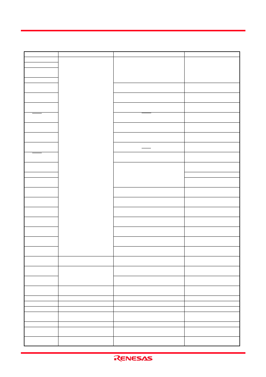
Table 10
Termination of unused pins
Pin
Termination 1
Termination 2
Termination 3
P00/SEG8
P07/SEG15 I/O port
When selecting SEG output, open.
P10/SEG16
P17/SEG23
P20/SEG0/(KW4)
P27/SEG7
P30/SEG24
P37/SEG31
P40/RXD
When selecting RxD function, perform
termination of input port.
P41/TXD
When selecting TxD function, perform
termination of output port.
P42/SCLK1
When selecting external clock input,
perform termination of input port.
When selecting internal clock output,
perform termination of output port.
P43/SRDY1
When selecting SRDY1 function, perform
termination of output port.
P44/SIN2/(KW0)
When selecting SIN2 function, perform
termination of input port.
P45/SOUT2/(KW1)
When selecting SOUT2 function, perform
termination of output port.
P46/SCLK2/(KW2)
When selecting external clock input,
perform termination of output port.
When selecting internal clock output,
perform termination of output port.
P47/SRDY2/(KW3)
When selecting SRDY2 function, perform
termination of output port.
P50/AN0/RTP0
P51/AN1/RTP1
When selecting AN function, these pins
can be opened. (A/D conversion result
cannot be guaranteed.)
When selecting RTP function,
perform termination of output port.
P52/AN2
P56/AN6
P57/AN7/ADKEY0
When selecting ADKEY function,
pull-up this pin through a resistor.
P60/XCIN
P61/XCOUT
Do not select XCIN
XCOUT oscillation
function by program.
P62/INT00/(LED0)
When selecting INT function,
perform termination of input port.
P63/TXOUT2/(LED1)
When selecting TXOUT function, perform
termination of output port.
P64/INT2/(LED2)
When selecting INT function,
perform termination of input port.
P65/TXOUT1/(LED3)
When selecting TXOUT function, perform
termination of output port.
P66/INT10/CNTR0/
(LED4)
When selecting CNTR input function or INT
function, perform termination of input port.
P67/CNTR1/(LED5)
When selecting CNTR input function,
perform termination of input port.
P70/C1/INT01
P71/C2/INT11
Disable the voltage multiplier, and
connect to VSS through a resistor.
When selecting INT function, disable the voltage
multiplier, and connect to VSS through a resistor.
P72/T2OUT/CKOUT
I/O port
When selecting T2OUT function or CKOUT
function, perform termination of output port.
P73/PWM0/T3OUT
P74/PWM1/T4OUT
When selecting PWM, T3OUT, or T4OUT
function, perform termination of output port.
VL3
Set the VL3 connect bit to “1” and
apply a Vcc level voltage to VL3 pin.
Set the VL3 connect bit to “0” and leave the
VL3 pin open.
VL2
VL3 ≥ VL2 ≥ VL1
VL1
Connect to VSS
COM0
COM3
Open
COM4/SEG35
COM7/SEG32
Open
VREF
Connect to VCC
XIN
When only on-chip oscillator is used,
connect to VCC through a resistor.
XOUT
When external clock is input or when
only on-chip oscillator is used, open.
相关PDF资料 |
PDF描述 |
|---|---|
| MC6805S3P | 8-BIT, MROM, MICROCONTROLLER, PDIP28 |
| MC908QT1AVDWE | 8-BIT, FLASH, 8 MHz, MICROCONTROLLER, PDSO8 |
| MC908QY4AVDT | 8-BIT, FLASH, 8 MHz, MICROCONTROLLER, PDSO16 |
| MC9S08AW16CFUE | 8-BIT, FLASH, 40 MHz, MICROCONTROLLER, PQFP64 |
| M902-01-156.2500LF | 156.25 MHz, OTHER CLOCK GENERATOR, CQCC36 |
相关代理商/技术参数 |
参数描述 |
|---|---|
| M38D59T-RLFS | 功能描述:BOARD EMULATOR FOR 38D5 GROUP RoHS:否 类别:编程器,开发系统 >> 内电路编程器、仿真器以及调试器 系列:- 产品变化通告:Development Systems Discontinuation 19/Jul/2010 标准包装:1 系列:* 类型:* 适用于相关产品:* 所含物品:* |
| M38DC-15 | 制造商:M/A-COM Technology Solutions 功能描述:MIXER(SPEC UX1015) - Bulk |
| M38K00F1-16FP | 制造商:MITSUBISHI 制造商全称:Mitsubishi Electric Semiconductor 功能描述:SINGLE-CHIP 8-BIT CMOS MICROCOMPUTER |
| M38K00F1-16HP | 制造商:MITSUBISHI 制造商全称:Mitsubishi Electric Semiconductor 功能描述:SINGLE-CHIP 8-BIT CMOS MICROCOMPUTER |
| M38K00F1-32FP | 制造商:MITSUBISHI 制造商全称:Mitsubishi Electric Semiconductor 功能描述:SINGLE-CHIP 8-BIT CMOS MICROCOMPUTER |
发布紧急采购,3分钟左右您将得到回复。