- 您现在的位置:买卖IC网 > PDF目录29118 > MC100ES6111FAR2 (MOTOROLA INC) 100E SERIES, LOW SKEW CLOCK DRIVER, 10 TRUE OUTPUT(S), 0 INVERTED OUTPUT(S), PQFP32 PDF资料下载
参数资料
| 型号: | MC100ES6111FAR2 |
| 厂商: | MOTOROLA INC |
| 元件分类: | 时钟及定时 |
| 英文描述: | 100E SERIES, LOW SKEW CLOCK DRIVER, 10 TRUE OUTPUT(S), 0 INVERTED OUTPUT(S), PQFP32 |
| 封装: | PLASTIC, LQFP-32 |
| 文件页数: | 7/7页 |
| 文件大小: | 109K |
| 代理商: | MC100ES6111FAR2 |
7
MC100ES6111
MOTOROLA ADVANCED CLOCK DRIVERS DEVICE DATA
683
APPLICATIONS INFORMATION
Understanding the junction temperature range of the
MC100ES6111
To make the optimum use of high clock frequency and low
skew capabilities of the MC100ES6111, the MC100ES6111 is
specified, characterized and tested for the junction tempera-
ture range of TJ=0°C to +110°C. Because the exact thermal
performance depends on the PCB type, design, thermal man-
agement and natural or forced air convection, the junction tem-
perature provides an exact way to correlate the application
specific conditions to the published performance data of this
datasheet. The correlation of the junction temperature range to
the application ambient temperature range and vice versa can
be done by calculation:
TJ = TA + Rthja Ptot
Assuming a thermal resistance (junction to ambient) of
54.4
°C/W (2s2p board, 200 ft/min airflow, see table 4) and a
typical power consumption of 610 mW (all outputs terminated
50 ohms to VTT, VCC=3.3V, frequency independent), the junc-
tion temperature of the MC100ES6111 is approximately
TA + 33 °C, and the minimum ambient temperature in this ex-
ample case calculates to -33
°C (the maximum ambient tem-
perature is 77
°C. See Table 8). Exceeding the minimum junc-
tion temperature specification of the MC100ES6111 does not
have a significant impact on the device functionality. However,
the continuous use the MC100ES6111 at high ambient temper-
atures requires thermal management to not exceed the speci-
fied maximum junction temperature. Please see the applica-
tion note AN1545 for a power consumption calculation
guideline.
Table 8: Ambient temperature ranges (Ptot = 610 mW)
Rthja (2s2p board)
TA, mina
TA, max
Natural convection
59.0
°C/W
-36
°C
74
°C
100 ft/min
54.4
°C/W
-33
°C
77
°C
200 ft/min
52.5
°C/W
-32
°C
78
°C
400 ft/min
50.4
°C/W
-30
°C
79
°C
800 ft/min
47.8
°C/W
-29
°C
81
°C
a. The MC100ES6111 device function is guaranteed from TA=-40 °C to
TJ=110 °C
Maintaining Lowest Device Skew
The MC100ES6111 guarantees low output-to-output bank
skew of 35 ps and a part-to-part skew of max. 250 ps. To en-
sure low skew clock signals in the application, both outputs of
any differential output pair need to be terminated identically,
even if only one output is used. When fewer than all nine out-
put pairs are used, identical termination of all output pairs with-
in the output bank is recommended. If an entire output bank is
not used, it is recommended to leave all of these outputs open
and unterminated. This will reduce the device power consump-
tion while maintaining minimum output skew.
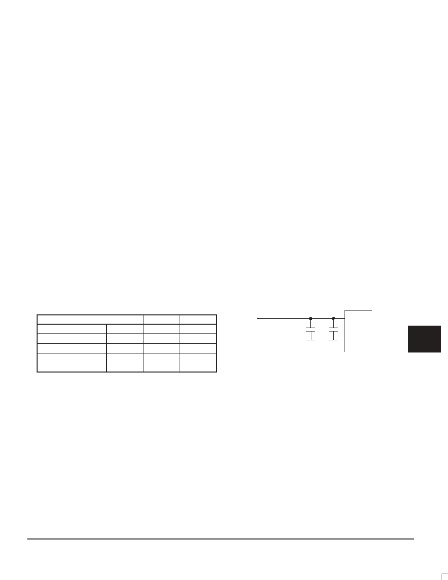
Power Supply Bypassing
The MC100ES6111 is a mixed analog/digital product. The
differential architecture of the MC100ES6111 supports low
noise signal operation at high frequencies. In order to maintain
its superior signal quality, all VCC pins should be bypassed by
high-frequency ceramic capacitors connected to GND. If the
spectral frequencies of the internally generated switching
noise on the supply pins cross the series resonant point of an
individual bypass capacitor, its overall impedance begins to
look inductive and thus increases with increasing frequency.
The parallel capacitor combination shown ensures that a low
impedance path to ground exists for frequencies well above
the noise bandwidth.
Figure 2. VCC Power Supply Bypass
VCC
MC100ES6111
VCC
33...100 nF
0.1 nF
相关PDF资料 |
PDF描述 |
|---|---|
| MC100ES6111FA | 100E SERIES, LOW SKEW CLOCK DRIVER, 10 TRUE OUTPUT(S), 0 INVERTED OUTPUT(S), PQFP32 |
| MC100ES6139DWR2 | 100E SERIES, LOW SKEW CLOCK DRIVER, 4 TRUE OUTPUT(S), 0 INVERTED OUTPUT(S), PDSO20 |
| MC100ES6220TBR2 | 100E SERIES, LOW SKEW CLOCK DRIVER, 10 TRUE OUTPUT(S), 0 INVERTED OUTPUT(S), PQFP52 |
| MC100ES6221AER2 | 100E SERIES, LOW SKEW CLOCK DRIVER, 20 TRUE OUTPUT(S), 0 INVERTED OUTPUT(S), PQFP52 |
| MC100ES6221AE | 100E SERIES, LOW SKEW CLOCK DRIVER, 20 TRUE OUTPUT(S), 0 INVERTED OUTPUT(S), PQFP52 |
相关代理商/技术参数 |
参数描述 |
|---|---|
| MC100ES6130DT | 功能描述:时钟驱动器及分配 Buffer RoHS:否 制造商:Micrel 乘法/除法因子:1:4 输出类型:Differential 最大输出频率:4.2 GHz 电源电压-最大: 电源电压-最小:5 V 最大工作温度:+ 85 C 封装 / 箱体:SOIC-8 封装:Reel |
| MC100ES6130EJ | 功能描述:时钟缓冲器 FSL 1-10 Diff LVPECL Fanout Buffer RoHS:否 制造商:Texas Instruments 输出端数量:5 最大输入频率:40 MHz 传播延迟(最大值): 电源电压-最大:3.45 V 电源电压-最小:2.375 V 最大功率耗散: 最大工作温度:+ 85 C 最小工作温度:- 40 C 封装 / 箱体:LLP-24 封装:Reel |
| MC100ES6130EJR2 | 功能描述:时钟缓冲器 FSL 1-10 Diff LVPECL Fanout Buffer RoHS:否 制造商:Texas Instruments 输出端数量:5 最大输入频率:40 MHz 传播延迟(最大值): 电源电压-最大:3.45 V 电源电压-最小:2.375 V 最大功率耗散: 最大工作温度:+ 85 C 最小工作温度:- 40 C 封装 / 箱体:LLP-24 封装:Reel |
| MC100ES6139DT | 功能描述:时钟发生器及支持产品 Buffer RoHS:否 制造商:Silicon Labs 类型:Clock Generators 最大输入频率:14.318 MHz 最大输出频率:166 MHz 输出端数量:16 占空比 - 最大:55 % 工作电源电压:3.3 V 工作电源电流:1 mA 最大工作温度:+ 85 C 安装风格:SMD/SMT 封装 / 箱体:QFN-56 |
| MC100ES6139EJ | 功能描述:时钟发生器及支持产品 FSL 1-4 LVPECL Div. 2/4, Div. 4/5/6 Cloc RoHS:否 制造商:Silicon Labs 类型:Clock Generators 最大输入频率:14.318 MHz 最大输出频率:166 MHz 输出端数量:16 占空比 - 最大:55 % 工作电源电压:3.3 V 工作电源电流:1 mA 最大工作温度:+ 85 C 安装风格:SMD/SMT 封装 / 箱体:QFN-56 |
发布紧急采购,3分钟左右您将得到回复。