- 您现在的位置:买卖IC网 > PDF目录15270 > LTC1266ACS#TR (Linear Technology)IC REG CTRLR BST PWM CM 16-SOIC PDF资料下载
参数资料
| 型号: | LTC1266ACS#TR |
| 厂商: | Linear Technology |
| 文件页数: | 6/20页 |
| 文件大小: | 0K |
| 描述: | IC REG CTRLR BST PWM CM 16-SOIC |
| 标准包装: | 2,500 |
| PWM 型: | 电流模式 |
| 输出数: | 1 |
| 频率 - 最大: | 400kHz |
| 占空比: | 100% |
| 电源电压: | 3.5 V ~ 18 V |
| 降压: | 是 |
| 升压: | 是 |
| 回扫: | 无 |
| 反相: | 无 |
| 倍增器: | 无 |
| 除法器: | 无 |
| Cuk: | 无 |
| 隔离: | 无 |
| 工作温度: | 0°C ~ 70°C |
| 封装/外壳: | 16-SOIC(0.154",3.90mm 宽) |
| 包装: | 带卷 (TR) |
�� �
�
�LTC1266�
�LTC1266-3.3/LTC1266-5�
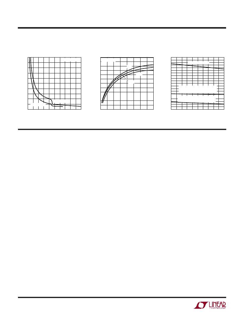
�TYPICAL� PERFOR� A� CE� CHARACTERISTICS�
�Operating� Frequency�
�Off-Time� vs� Output� Voltage�
�vs� (V� IN� –� V� OUT� )� Voltage�
�Current� Sense� Threshold� Voltage�
�100�
�80�
�V� SENSE� –� =� V� OUT�
�3.0�
�2.5�
�V� OUT� = 3.3V�
�0� °� C�
�200�
�150�
�MAX THRESHOLD�
�60�
�2.0�
�1.5�
�25� °� C�
�70� °� C�
�100�
�40�
�1.0�
�50�
�MIN� THRESHOLD� (Burst� Mode�
�OPERATION� ENABLED)�
�20�
�LTC1266-5�
�0.5�
�0�
�MIN� THRESHOLD� (Burst� Mode�
�OPERATION� INHIBIT)�
�LTC1266-3.3�
�0�
�0�
�1�
�2�
�3� 4�
�5�
�0�
�0�
�2�
�4�
�6�
�8�
�10�
�12�
�14�
�16�
�–50�
�0�
�20�
�40�
�60�
�80�
�100�
�OUTPUT� VOLTAGE� (V)�
�PI� FU� CTIO� S�
�1266� G10�
�(V� IN� –� V� OUT� )� VOLTAGE� (V)�
�1266� G11�
�TEMPERATURE� (� °� C)�
�1266� G12�
�TDRIVE� (Pin� 1):� High� Current� Drive� for� Topside� MOSFET.�
�This� MOSFET� can� be� either� P-channel� or� N-channel,� user�
�selectable� by� Pin� 3.� Voltage� swing� at� this� pin� is� from� PWR�
�V� IN� to� ground.�
�PWR� V� IN� (Pin� 2):� Power� Suppy� for� Drive� Signals.� Must� be�
�closely� decoupled� to� power� ground� (Pin� 15).�
�PINV� (Pin� 3):� Phase� Invert.� Sets� the� phase� of� the� topside�
�driver� to� drive� either� a� P-channel� or� an� N-channel� MOSFET�
�as� follows:�
�P-channel:� Pin� 3� =� 0V�
�N-channel:� Pin� 3� =� PWR� V� IN�
�BINH� (Pin� 4):� Burst� Mode� Operation� Inhibit.� A� CMOS� logic�
�high� on� this� pin� will� disable� the� Burst� Mode� operation�
�feature� forcing� continuous� operation� down� to� zero� load.�
�V� IN� (Pin� 5):� Main� Supply� Pin.�
�C� T� (Pin� 6):� External� Capacitor.� C� T� from� Pin� 4� to� ground� sets�
�the� operating� frequency.� The� actual� frequency� is� also�
�dependent� on� the� input� voltage.�
�I� TH� (Pin� 7):� Gain� Amplifier� Decoupling� Point.� The� current�
�comparator� threshold� increases� with� the� Pin� 7� voltage.�
�SENSE� –� (Pin� 8):� Connects� to� internal� resistive� divider�
�which� sets� the� output� voltage� in� LTC1266-3.3� and�
�LTC1266-5� versions.� Pin� 8� is� also� the� (–)� input� for� the�
�current� comparator.�
�6�
�SENSE� +� (Pin� 9):� The� (+)� Input� to� the� Current� Comparator.�
�A� built-in� offset� between� Pins� 8� and� 9� in� conjunction� with�
�R� SENSE� sets� the� current� trip� threshold.�
�V� FB� (Pin� 10):� For� the� LTC1266� adjustable� version,� Pin� 10�
�serves� as� the� feedback� pin� from� an� external� resistive�
�divider� used� to� set� the� output� voltage.� On� LTC1266-3.3�
�and� LTC1266-5� versions� this� pin� is� not� used.�
�SHDN� (Pin� 11):� When� grounded,� the� LTC1266� series�
�operates� normally.� Pulling� Pin� 11� high� holds� both�
�MOSFETs� off� and� puts� the� LTC1266� in� micropower� shut-�
�down� mode.� Requires� CMOS� logic� signal� with� t� r� ,� t� f� <� 1� μ� s.�
�Should� not� be� left� floating.�
�SGND� (Pin� 12):� Small-Signal� Ground.� Must� be� routed�
�separately� from� other� grounds� to� the� (–)� terminal� of� C� OUT� .�
�LB� IN� (Pin� 13):� Input� to� the� Low-Battery� Comparator.� This�
�input� is� compared� to� an� internal� 1.25V� reference.�
�LB� OUT� (Pin� 14):� Open� Drain� Output� of� the� Low-Battery�
�Comparator.� This� pin� will� sink� current� when� Pin� 13� is�
�below� 1.25V.�
�PGND� (Pin� 15):� Driver� Power� Ground.� Connects� to� source�
�of� N-channel� MOSFET� and� the� (–)� terminal� of� C� IN� .�
�BDRIVE� (Pin� 16):� High� Current� Drive� for� Bottom�
�N-Channel� MOSFET.� Voltage� swing� at� Pin� 16� is� from�
�ground� to� PWR� V� IN� .�
�相关PDF资料 |
PDF描述 |
|---|---|
| LTC1625CGN#TRPBF | IC REG CTRLR BUCK PWM CM 16-SSOP |
| LTC1625CGN#TR | IC REG CTRLR BUCK PWM CM 16-SSOP |
| LTC3891HUDC#TRPBF | IC REG CTRLR BUCK PWM CM 20-QFN |
| LTC3709EG#PBF | IC REG CTRLR BUCK PWM CM 36-SSOP |
| LTC3709EUH#PBF | IC REG CTRLR BUCK PWM CM 32-QFN |
相关代理商/技术参数 |
参数描述 |
|---|---|
| MC10E404FNR2G | 功能描述:逻辑门 5V ECL Quad Diff AND/NAND RoHS:否 制造商:Texas Instruments 产品:OR 逻辑系列:LVC 栅极数量:2 线路数量(输入/输出):2 / 1 高电平输出电流:- 16 mA 低电平输出电流:16 mA 传播延迟时间:3.8 ns 电源电压-最大:5.5 V 电源电压-最小:1.65 V 最大工作温度:+ 125 C 安装风格:SMD/SMT 封装 / 箱体:DCU-8 封装:Reel |
| MC10E411FN | 功能描述:时钟缓冲器 5V PECL/NECL RAMBus RoHS:否 制造商:Texas Instruments 输出端数量:5 最大输入频率:40 MHz 传播延迟(最大值): 电源电压-最大:3.45 V 电源电压-最小:2.375 V 最大功率耗散: 最大工作温度:+ 85 C 最小工作温度:- 40 C 封装 / 箱体:LLP-24 封装:Reel |
| MC10E411FNG | 功能描述:时钟缓冲器 5V PECL/NECL RAMBus 1:9 时钟缓冲器 RoHS:否 制造商:Texas Instruments 输出端数量:5 最大输入频率:40 MHz 传播延迟(最大值): 电源电压-最大:3.45 V 电源电压-最小:2.375 V 最大功率耗散: 最大工作温度:+ 85 C 最小工作温度:- 40 C 封装 / 箱体:LLP-24 封装:Reel |
| MC10E411FNR2 | 功能描述:时钟缓冲器 5V PECL/NECL RAMBus RoHS:否 制造商:Texas Instruments 输出端数量:5 最大输入频率:40 MHz 传播延迟(最大值): 电源电压-最大:3.45 V 电源电压-最小:2.375 V 最大功率耗散: 最大工作温度:+ 85 C 最小工作温度:- 40 C 封装 / 箱体:LLP-24 封装:Reel |
| MC10E411FNR2G | 功能描述:时钟缓冲器 5V PECL/NECL RAMBus 1:9 时钟缓冲器 RoHS:否 制造商:Texas Instruments 输出端数量:5 最大输入频率:40 MHz 传播延迟(最大值): 电源电压-最大:3.45 V 电源电压-最小:2.375 V 最大功率耗散: 最大工作温度:+ 85 C 最小工作温度:- 40 C 封装 / 箱体:LLP-24 封装:Reel |
发布紧急采购,3分钟左右您将得到回复。