- 您现在的位置:买卖IC网 > PDF目录16781 > V300C15E150BG3 (Vicor Corporation)CONVERTER MOD DC/DC 15V 150W PDF资料下载
参数资料
| 型号: | V300C15E150BG3 |
| 厂商: | Vicor Corporation |
| 文件页数: | 9/13页 |
| 文件大小: | 0K |
| 描述: | CONVERTER MOD DC/DC 15V 150W |
| 设计资源: | Maxi/Mini/Micro Design Guide, Appl Manual |
| 标准包装: | 1 |
| 系列: | 微型 |
| 类型: | 隔离 |
| 输出数: | 1 |
| 电压 - 输入(最小): | 180V |
| 电压 - 输入(最大): | 375V |
| Voltage - Output 1: | 15V |
| 电流 - 输出(最大): | * |
| 电源(瓦) - 制造商系列: | 150W |
| 电压 - 隔离: | * |
| 特点: | * |
| 安装类型: | 通孔 |
| 封装/外壳: | 模块 |
| 尺寸/尺寸: | 2.28" L x 1.45" W x 0.65" H(57.9mm x 36.8mm x 16.5mm) |
| 包装: | 散装 |
| 工作温度: | -10°C ~ 100°C |
| 效率: | * |
| 电源(瓦特)- 最大: | * |
�� �
�
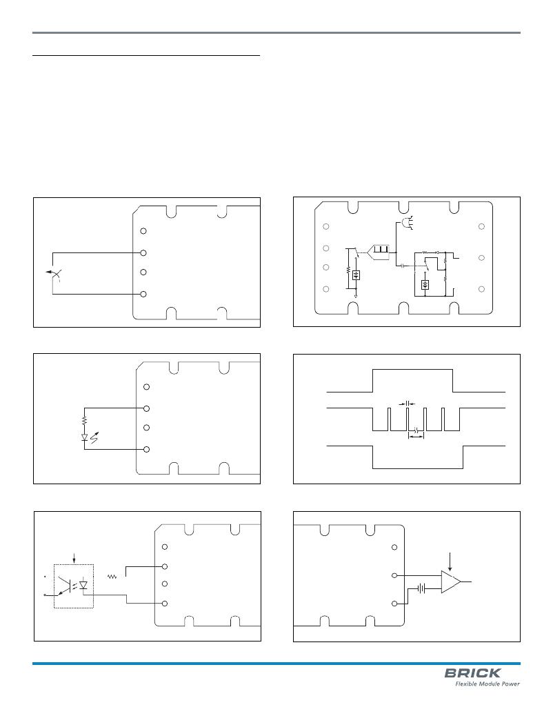
�300� V� Input�
�PRIMARY� CONTROL� -� PC� PIN�
�Module� Enable/Disable�
�The� module� may� be� disabled� by� pulling� PC� to� 0� V� (2.3� V�
�max)� with� respect� to� the� –Input.� This� may� be� done� with� an�
�open� collector� transistor,� relay,� or� optocoupler.� Converters�
�may� be� disabled� with� a� single� transistor� or� relay� either� directly�
�or� via� “OR’ing”� diodes� for� 2� or� more� converters.� See� Figure� 2.�
�Primary� Auxiliary� Supply�
�During� normal� operation� only,� the� PC� Pin� can� source� 5.7� V� @�
�1.5� mA.� In� the� example� shown� in� Figure� 4,� PC� powers� a� mod-�
�ule� enabled� LED.�
�Module� Alarm�
�The� module� contains� “watchdog”� circuitry� which� monitors�
�input� voltage,� operating� temperature� and� internal� operating�
�parameters.� In� the� event� that� any� of� these� parameters� are�
�outside� of� their� allowable� operating� range,� the� module� will�
�shut� down� and� PC� will� go� low.� PC� will� periodically� go� high�
�and� the� module� will� check� to� see� if� the� fault� (as� an� example,�
�Input� Undervoltage)� has� cleared.� If� the� fault� has� not� been�
�cleared,� PC� will� go� low� again� and� the� cycle� will� restart.� The�
�SC� pin� will� go� low� in� the� event� of� a� fault� and� return� to� its� nor-�
�mal� state� after� the� fault� has� been� cleared.� See� Figures� 3� and� 5.�
�Input� Undervoltage�
�Input� Overvoltage� [a]�
�+IN�
�+IN�
�Over� Temperature�
�Module� Faults�
�+OUT�
�Disable�
�PC�
�PR�
�–IN�
�PC�
�PR�
�1M�
�–IN�
�SW1�
�Auto�
�Restart�
�2-20� ms� typ.�
�f(V� IN� )�
�SW2�
�5.7� Vdc�
�(0-3� mA)�
�SW1,� 2,� &� 3� shown�
�in� "Fault"� position�
�50� Ω�
�SW3�
�1.23�
�Vdc�
�1K�
�6K�
�SC�
�–OUT�
�Figure� 2� —� Module� enable/disable.�
�Figure� 3� —� PC/SC� module� alarm� logic.�
�Not� applicable� for� 300� Vdc� Input� family�
�Disable = PC < 2.3 V�
�[a]�
�+IN�
�PC�
�Fault�
�PC�
�5.7� V�
�40� μs� typ.�
�"Module�
�Enabled"�
�4� k� Ω�
�PR�
�–IN�
�SC�
�1.23� V�
�2-20� ms� typ.�
�Figure� 4� —� LED� on-state� indicator.�
�Figure� 5� —� PC/SC� module� alarm� timing.�
�Optocoupler�
�+IN�
�+OUT�
�Comparator�
�PC�
�4k�
�PR�
�–IN�
�SC�
�–OUT�
�1.00� V�
�Alarm�
�Figure� 6� —� Isolated� on-state� indicator.�
�Figure� 7� —� Secondary� side� on-state� indicator.�
�300� V� Micro� Family�
�Page� 9� of� 13�
�Rev� 9.0�
�4/2013�
�vicorpower.com�
�800� 735.6200�
�相关PDF资料 |
PDF描述 |
|---|---|
| ECC10DRYH-S734 | CONN EDGECARD 20POS DIP .100 SLD |
| B78108T1183K | CHOKE RF 18UH 175MA AXIAL |
| H3CCS-2006M | IDC CABLE - HKC20S/AE20M/HKC20S |
| VERSAFIT-1/2-2-FSP | HEAT SHRINK TUBING |
| 202K163-12-0 | BOOT MOLDED |
相关代理商/技术参数 |
参数描述 |
|---|---|
| MC10EP131FAR2G | 功能描述:触发器 3.3V/5V ECL Quad D-Type RoHS:否 制造商:Texas Instruments 电路数量:2 逻辑系列:SN74 逻辑类型:D-Type Flip-Flop 极性:Inverting, Non-Inverting 输入类型:CMOS 输出类型: 传播延迟时间:4.4 ns 高电平输出电流:- 16 mA 低电平输出电流:16 mA 电源电压-最大:5.5 V 最大工作温度:+ 85 C 安装风格:SMD/SMT 封装 / 箱体:X2SON-8 封装:Reel |
| MC10EP131MNG | 功能描述:触发器 BBG ECL 4BIT RoHS:否 制造商:Texas Instruments 电路数量:2 逻辑系列:SN74 逻辑类型:D-Type Flip-Flop 极性:Inverting, Non-Inverting 输入类型:CMOS 输出类型: 传播延迟时间:4.4 ns 高电平输出电流:- 16 mA 低电平输出电流:16 mA 电源电压-最大:5.5 V 最大工作温度:+ 85 C 安装风格:SMD/SMT 封装 / 箱体:X2SON-8 封装:Reel |
| MC10EP131MNR4G | 功能描述:触发器 BBG ECL 4BIT RoHS:否 制造商:Texas Instruments 电路数量:2 逻辑系列:SN74 逻辑类型:D-Type Flip-Flop 极性:Inverting, Non-Inverting 输入类型:CMOS 输出类型: 传播延迟时间:4.4 ns 高电平输出电流:- 16 mA 低电平输出电流:16 mA 电源电压-最大:5.5 V 最大工作温度:+ 85 C 安装风格:SMD/SMT 封装 / 箱体:X2SON-8 封装:Reel |
| MC10EP139DT | 功能描述:时钟发生器及支持产品 3.3V/5V ECL Clock RoHS:否 制造商:Silicon Labs 类型:Clock Generators 最大输入频率:14.318 MHz 最大输出频率:166 MHz 输出端数量:16 占空比 - 最大:55 % 工作电源电压:3.3 V 工作电源电流:1 mA 最大工作温度:+ 85 C 安装风格:SMD/SMT 封装 / 箱体:QFN-56 |
| MC10EP139DTG | 功能描述:时钟发生器及支持产品 3.3V/5V ECL Clock Generator RoHS:否 制造商:Silicon Labs 类型:Clock Generators 最大输入频率:14.318 MHz 最大输出频率:166 MHz 输出端数量:16 占空比 - 最大:55 % 工作电源电压:3.3 V 工作电源电流:1 mA 最大工作温度:+ 85 C 安装风格:SMD/SMT 封装 / 箱体:QFN-56 |
发布紧急采购,3分钟左右您将得到回复。