参数资料
| 型号: | MC7410TVU400LE |
| 厂商: | Freescale Semiconductor |
| 文件页数: | 13/56页 |
| 文件大小: | 0K |
| 描述: | MPU RISC 32BIT 360-CBGA |
| 标准包装: | 44 |
| 系列: | MPC74xx |
| 处理器类型: | 32-位 MPC74xx PowerPC |
| 速度: | 400MHz |
| 电压: | 1.8V |
| 安装类型: | 表面贴装 |
| 封装/外壳: | 360-BCBGA,FCCBGA |
| 供应商设备封装: | 360-FCCBGA(25x25) |
| 包装: | 托盘 |
第1页第2页第3页第4页第5页第6页第7页第8页第9页第10页第11页第12页当前第13页第14页第15页第16页第17页第18页第19页第20页第21页第22页第23页第24页第25页第26页第27页第28页第29页第30页第31页第32页第33页第34页第35页第36页第37页第38页第39页第40页第41页第42页第43页第44页第45页第46页第47页第48页第49页第50页第51页第52页第53页第54页第55页第56页
MPC7410 RISC Microprocessor Hardware Specifications, Rev. 6.1
20
Freescale Semiconductor
Electrical and Thermal Characteristics
4.2.4
L2 Bus AC Specifications
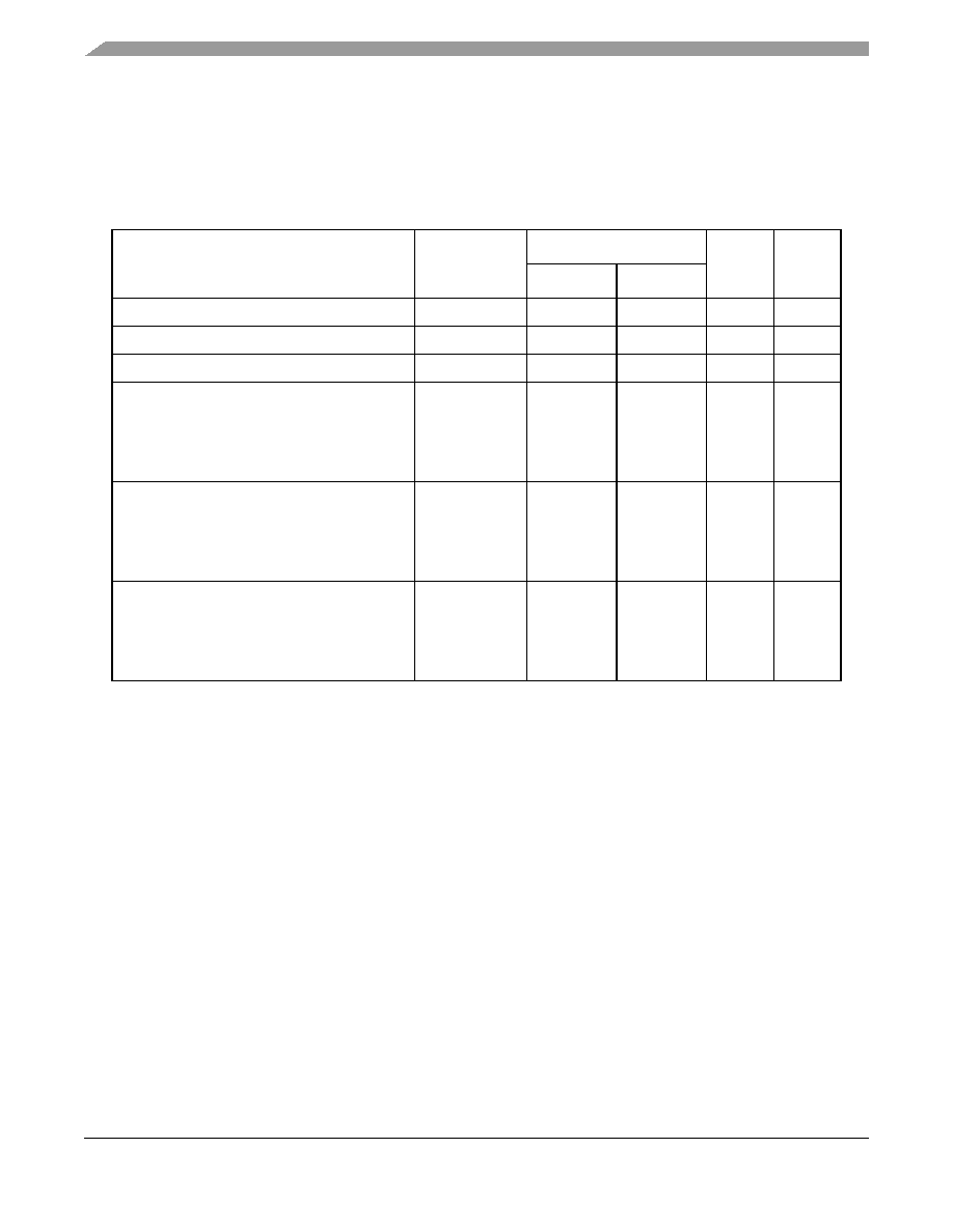
Table 10 provides the L2 bus interface AC timing specifications for the MPC7410 as defined in Figure 8 and
Table 10. L2 Bus Interface AC Timing Specifications
At recommended operating conditions (see Table 3)
Parameter
Symbol
400, 450, 500 MHz
Unit
Notes
Min
Max
L2SYNC_IN rise and fall time
tL2CR and tL2CF
—1.0
ns
1
Setup times: Data and parity
tDVL2CH
1.5
—
ns
2
Input hold times: Data and parity
tDXL2CH
—0.0
ns
2
Valid times:
All outputs when L2CR[14–15] = 00
All outputs when L2CR[14–15] = 01
All outputs when L2CR[14–15] = 10
All outputs when L2CR[14–15] = 11
tL2CHOV
—
2.5
2.9
3.5
ns
3, 4
Output hold times
All outputs when L2CR[14–15] = 00
All outputs when L2CR[14–15] = 01
All outputs when L2CR[14–15] = 10
All outputs when L2CR[14–15] = 11
tL2CHOX
0.4
0.8
1.2
1.6
—
ns
3
L2SYNC_IN to high impedance:
All outputs when L2CR[14–15] = 00
All outputs when L2CR[14–15] = 01
All outputs when L2CR[14–15] = 10
All outputs when L2CR[14–15] = 11
tL2CHOZ
—
2.0
2.5
3.0
3.5
ns
—
Notes:
1. Rise and fall times for the L2SYNC_IN input are measured from 20% to 80% of L2OVDD.
2. All input specifications are measured from the midpoint of the signal in question to the midpoint voltage of the rising
edge of the input L2SYNC_IN (see Figure 8). Input timings are measured at the pins.
3. All output specifications are measured from the midpoint voltage of the rising edge of L2SYNC_IN to the midpoint
of the signal in question. The output timings are measured at the pins. All output timings assume a purely resistive
50-
Ω load (see Figure 10).
4. The outputs are valid for both single-ended and differential L2CLK modes. For pipelined registered synchronous
BurstRAMs, L2CR[14–15] = 00 is recommended. For pipelined late write synchronous BurstRAMs,
L2CR[14–15] = 10 is recommended.
相关PDF资料 |
PDF描述 |
|---|---|
| IDT71T75802S166BGI8 | IC SRAM 18MBIT 166MHZ 119BGA |
| FMC35DRAI | CONN EDGECARD 70POS R/A .100 SLD |
| MPC8567EVTAQGG | MPU POWERQUICC III 1023-PBGA |
| IDT71T75802S166BGGI8 | IC SRAM 18MBIT 166MHZ 119BGA |
| FMM43DSEF-S13 | CONN EDGECARD 86POS .156 EXTEND |
相关代理商/技术参数 |
参数描述 |
|---|---|
| MC7410VU400LE | 功能描述:微处理器 - MPU REV 1.4 105C PB FREE RoHS:否 制造商:Atmel 处理器系列:SAMA5D31 核心:ARM Cortex A5 数据总线宽度:32 bit 最大时钟频率:536 MHz 程序存储器大小:32 KB 数据 RAM 大小:128 KB 接口类型:CAN, Ethernet, LIN, SPI,TWI, UART, USB 工作电源电压:1.8 V to 3.3 V 最大工作温度:+ 85 C 安装风格:SMD/SMT 封装 / 箱体:FBGA-324 |
| MC7410VU400NE | 功能描述:微处理器 - MPU NITRO RV 1.4 ROHS RoHS:否 制造商:Atmel 处理器系列:SAMA5D31 核心:ARM Cortex A5 数据总线宽度:32 bit 最大时钟频率:536 MHz 程序存储器大小:32 KB 数据 RAM 大小:128 KB 接口类型:CAN, Ethernet, LIN, SPI,TWI, UART, USB 工作电源电压:1.8 V to 3.3 V 最大工作温度:+ 85 C 安装风格:SMD/SMT 封装 / 箱体:FBGA-324 |
| MC7410VU450NE | 功能描述:微处理器 - MPU NITRO RV 1.4 ROHS RoHS:否 制造商:Atmel 处理器系列:SAMA5D31 核心:ARM Cortex A5 数据总线宽度:32 bit 最大时钟频率:536 MHz 程序存储器大小:32 KB 数据 RAM 大小:128 KB 接口类型:CAN, Ethernet, LIN, SPI,TWI, UART, USB 工作电源电压:1.8 V to 3.3 V 最大工作温度:+ 85 C 安装风格:SMD/SMT 封装 / 箱体:FBGA-324 |
| MC7410VU500LE | 功能描述:微处理器 - MPU REV 1.4 105C PB FREE RoHS:否 制造商:Atmel 处理器系列:SAMA5D31 核心:ARM Cortex A5 数据总线宽度:32 bit 最大时钟频率:536 MHz 程序存储器大小:32 KB 数据 RAM 大小:128 KB 接口类型:CAN, Ethernet, LIN, SPI,TWI, UART, USB 工作电源电压:1.8 V to 3.3 V 最大工作温度:+ 85 C 安装风格:SMD/SMT 封装 / 箱体:FBGA-324 |
| MC7411MEL | 制造商:Rochester Electronics LLC 功能描述:- Bulk |
发布紧急采购,3分钟左右您将得到回复。