- 您现在的位置:买卖IC网 > PDF目录80382 > MCF53017CMJ240J (FREESCALE SEMICONDUCTOR INC) MICROPROCESSOR, PBGA256 PDF资料下载
参数资料
| 型号: | MCF53017CMJ240J |
| 厂商: | FREESCALE SEMICONDUCTOR INC |
| 元件分类: | 微控制器/微处理器 |
| 英文描述: | MICROPROCESSOR, PBGA256 |
| 封装: | 17 X 17 MM, ROHS COMPLIANT, PLASTIC, MAPBGA-256 |
| 文件页数: | 24/62页 |
| 文件大小: | 2365K |
| 代理商: | MCF53017CMJ240J |
第1页第2页第3页第4页第5页第6页第7页第8页第9页第10页第11页第12页第13页第14页第15页第16页第17页第18页第19页第20页第21页第22页第23页当前第24页第25页第26页第27页第28页第29页第30页第31页第32页第33页第34页第35页第36页第37页第38页第39页第40页第41页第42页第43页第44页第45页第46页第47页第48页第49页第50页第51页第52页第53页第54页第55页第56页第57页第58页第59页第60页第61页第62页
MCF5301x Data Sheet, Rev. 5
Preliminary—Subject to Change Without Notice
Preliminary Electrical Characteristics
Freescale Semiconductor
30
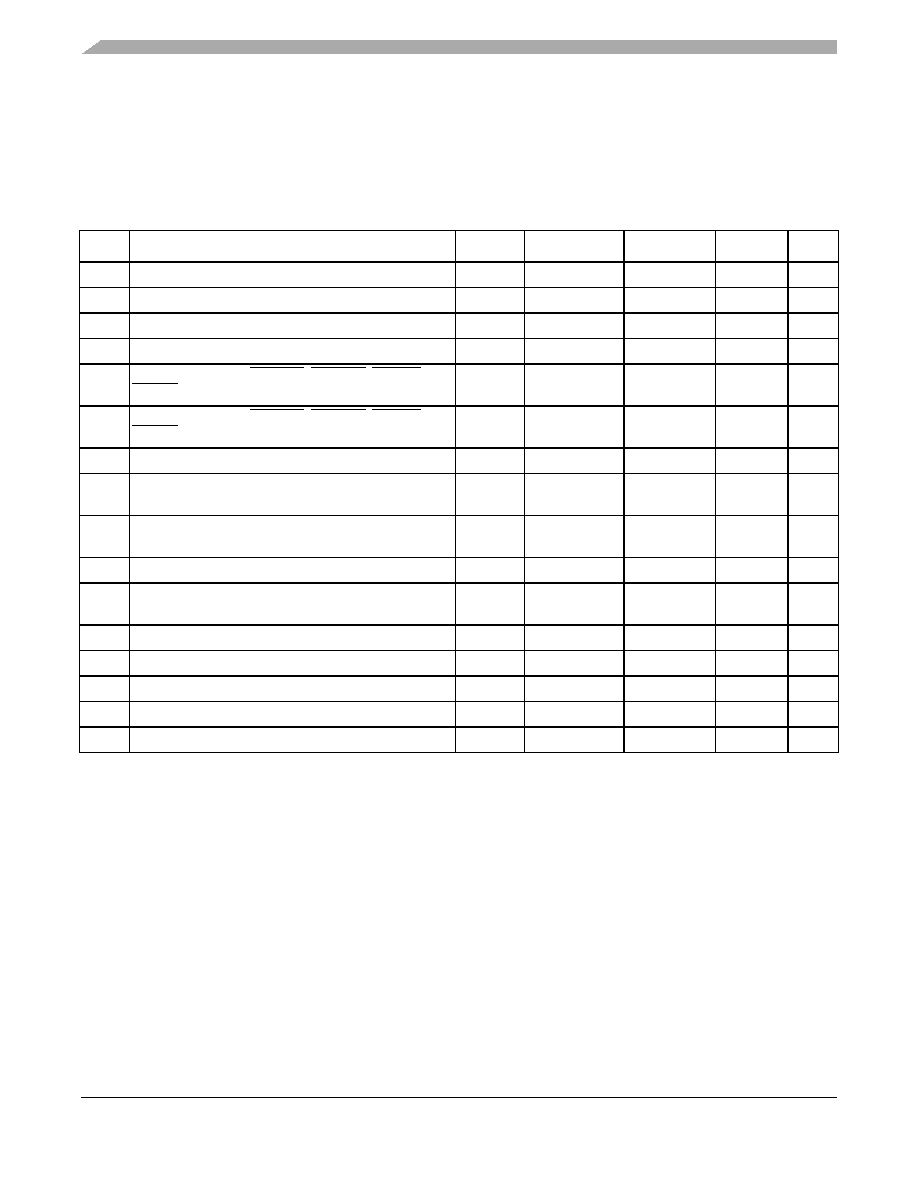
5.7.2
DDR SDRAM AC Timing Characteristics
When the SDRAM controller is configured for DDR SDRAM, the following timing numbers must be followed to properly latch
or drive data onto the memory bus. All timing numbers are relative to the four DQS byte lanes. The following timing numbers
are subject to change at anytime, and are only provided to aid in early board design.
Table 14. DDR Timing Specifications
Num
Characteristic
Symbol
Min
Max
Unit
Notes
Frequency of Operation
tDDCK
50
80
Mhz
1
1 The frequency of operation is either 2x or 4x the FB_CLK frequency of operation. FlexBus and SDRAM clock operate at the
same frequency as the internal bus clock.
DD1
Clock Period
tDDSK
12.5
20
ns
2
2 SD_CLK is one SDRAM clock in (ns).
DD2
Pulse Width High
tDDCKH
0.45
0.55
SD_CLK
3
3 Pulse width high plus pulse width low cannot exceed min and max clock period.
DD3
Pulse Width Low
tDDCKL
0.45
0.55
SD_CLK
DD4
Address, SD_CKE, SD_CAS, SD_RAS, SD_WE,
SD_CS[1:0] Output Valid
tSDCHACV
—0.5
× SD_CLK
+1.0
ns
4
4 Command output valid should be 1/2 the memory bus clock (SD_CLK) plus some minor adjustments for process, temperature,
and voltage variations.
DD5
Address, SD_CKE, SD_CAS, SD_RAS, SD_WE,
SD_CS[1:0] Output Hold
tSDCHACI
2.0
—
ns
DD6
Write Command to first DQS Latching Transition
tCMDVDQ
—
1.25
SD_CLK
DD7
Data and Data Mask Output Setup (DQ-->DQS)
Relative to DQS (DDR Write Mode)
tDQDMV
1.5
—
ns
5
6
5 This specification relates to the required input setup time of today’s DDR memories. The device’s output setup should be larger
than the input setup of the DDR memories. If it is not larger, then the input setup on the memory will be in violation.
SD_D[31:24] is relative to SD_DQS3, SD_D[23:16] is relative to SD_DQS2, SD_D[15:8] is relative to SD_DQS1, and
SD_D[7:0] is relative SD_DQS0.
6 The first data beat will be valid before the first rising edge of DQS and after the DQS write preamble. The remaining data beats
will be valid for each subsequent DQS edge.
DD8
Data and Data Mask Output Hold (DQS-->DQ)
Relative to DQS (DDR Write Mode)
tDQDMI
1.0
—
ns
7
7 This specification relates to the required hold time of today’s DDR memories. SD_D[31:24] is relative to SD_DQS3,
SD_D[23:16] is relative to SD_DQS2, SD_D[15:8] is relative to SD_DQS1, and SD_D[7:0] is relative SD_DQS0.
DD9
Input Data Skew Relative to DQS (Input Setup)
tDVDQ
—1
ns
8
DD10 Input Data Hold Relative to DQS.
tDIDQ
0.25
× SD_CLK
+0.5ns
—ns
9
DD11 DQS falling edge from SDCLK rising (output hold time) tDQLSDCH
0.5
—
ns
DD12 DQS input read preamble width
tDQRPRE
0.9
1.1
SD_CLK
DD13 DQS input read postamble width
tDQRPST
0.4
0.6
SD_CLK
DD14 DQS output write preamble width
tDQWPRE
0.25
—
SD_CLK
DD15 DQS output write postamble width
tDQWPST
0.4
0.6
SD_CLK
相关PDF资料 |
PDF描述 |
|---|---|
| MPC8544VTAQFB | 32-BIT, 1000 MHz, RISC PROCESSOR, PBGA783 |
| MPC8280VRBX | 32-BIT, 66 MHz, RISC PROCESSOR, PBGA516 |
| MPC8309VMAFDCA | 32-BIT, 333 MHz, RISC PROCESSOR, PBGA489 |
| MPC5604CF1MLQ6R | MICROCONTROLLER, PQFP144 |
| MCF51QH128VFM | FLASH, 50 MHz, MICROCONTROLLER, QCC32 |
相关代理商/技术参数 |
参数描述 |
|---|---|
| MCF5307 | 制造商:MOTOROLA 制造商全称:Motorola, Inc 功能描述:UART MODULE |
| MCF5307AI66B | 功能描述:微处理器 - MPU MCF5307 V3CORE 4KSRAM RoHS:否 制造商:Atmel 处理器系列:SAMA5D31 核心:ARM Cortex A5 数据总线宽度:32 bit 最大时钟频率:536 MHz 程序存储器大小:32 KB 数据 RAM 大小:128 KB 接口类型:CAN, Ethernet, LIN, SPI,TWI, UART, USB 工作电源电压:1.8 V to 3.3 V 最大工作温度:+ 85 C 安装风格:SMD/SMT 封装 / 箱体:FBGA-324 |
| MCF5307AI90B | 功能描述:微处理器 - MPU MCF5307 V3CORE 4KSRAM RoHS:否 制造商:Atmel 处理器系列:SAMA5D31 核心:ARM Cortex A5 数据总线宽度:32 bit 最大时钟频率:536 MHz 程序存储器大小:32 KB 数据 RAM 大小:128 KB 接口类型:CAN, Ethernet, LIN, SPI,TWI, UART, USB 工作电源电压:1.8 V to 3.3 V 最大工作温度:+ 85 C 安装风格:SMD/SMT 封装 / 箱体:FBGA-324 |
| MCF5307AI90BB1 | 制造商:Rochester Electronics LLC 功能描述: 制造商:Freescale Semiconductor 功能描述: |
| MCF5307CAI66B | 功能描述:微处理器 - MPU MCF5307 V3CORE 4KSRAM RoHS:否 制造商:Atmel 处理器系列:SAMA5D31 核心:ARM Cortex A5 数据总线宽度:32 bit 最大时钟频率:536 MHz 程序存储器大小:32 KB 数据 RAM 大小:128 KB 接口类型:CAN, Ethernet, LIN, SPI,TWI, UART, USB 工作电源电压:1.8 V to 3.3 V 最大工作温度:+ 85 C 安装风格:SMD/SMT 封装 / 箱体:FBGA-324 |
发布紧急采购,3分钟左右您将得到回复。