- 您现在的位置:买卖IC网 > PDF目录3980 > IDT70V657S15BF (IDT, Integrated Device Technology Inc)IC SRAM 1.125MBIT 15NS 208FBGA PDF资料下载
参数资料
| 型号: | IDT70V657S15BF |
| 厂商: | IDT, Integrated Device Technology Inc |
| 文件页数: | 13/24页 |
| 文件大小: | 0K |
| 描述: | IC SRAM 1.125MBIT 15NS 208FBGA |
| 标准包装: | 7 |
| 格式 - 存储器: | RAM |
| 存储器类型: | SRAM - 双端口,异步 |
| 存储容量: | 1.125M(32K x 36) |
| 速度: | 15ns |
| 接口: | 并联 |
| 电源电压: | 3.15 V ~ 3.45 V |
| 工作温度: | 0°C ~ 70°C |
| 封装/外壳: | 208-LFBGA |
| 供应商设备封装: | 208-CABGA(15x15) |
| 包装: | 托盘 |
| 其它名称: | 70V657S15BF |
�� �
�
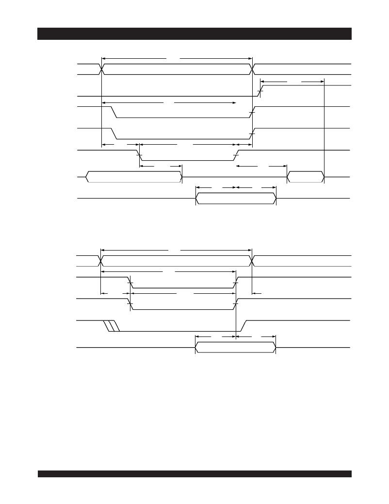
�IDT70V659/58/57S�
�High-Speed� 3.3V� 128/64/32K� x� 36� Asynchronous� Dual-Port� Static� RAM�
�Industrial� and� Commercial� Temperature� Ranges�
�Timing� Waveform� of� Write� Cycle� No.� 1,� R/� W� Controlled� Timing� (1,5,8)�
�t� WC�
�ADDRESS�
�OE�
�t� AW�
�t� HZ�
�(7)�
�CE� or� SEM�
�(9)�
�BE� n�
�(9)�
�t� AS� (6)�
�t� WP�
�(2)�
�t� WR�
�(3)�
�R/� W�
�t� WZ� (7)�
�t� OW�
�DATA� OUT�
�(4)�
�t� DW�
�t� DH�
�(4)�
�DATA� IN�
�4869� drw� 08�
�Timing� Waveform� of� Write� Cycle� No.� 2,� CE� Controlled� Timing� (1,5)�
�t� WC�
�ADDRESS�
�t� AW�
�CE� or� SEM�
�(9)�
�t� AS�
�BE� n�
�(9)�
�R/� W�
�DATA� IN�
�(6)�
�t� EW� (2)�
�t� DW�
�t� WR� (3)�
�t� DH�
�4869� drw� 09�
�.�
�NOTES:�
�1.� R/� W� or� CE� or� BE� n� =� V� IH� during� all� address� transitions.�
�2.� A� write� occurs� during� the� overlap� (t� EW� or� t� WP� )� of� a� CE� =� V� IL� and� a� R/� W� =� V� IL� for� memory� array� writing� cycle.�
�3.� t� WR� is� measured� from� the� earlier� of� CE� or� R/� W� (or� SEM� or� R/� W� )� going� HIGH� to� the� end� of� write� cycle.�
�4.� During� this� period,� the� I/O� pins� are� in� the� output� state� and� input� signals� must� not� be� applied.�
�5.� If� the� CE� or� SEM� =� V� IL� transition� occurs� simultaneously� with� or� after� the� R/� W� =� V� IL� transition,� the� outputs� remain� in� the� High-impedance� state.�
�6.� Timing� depends� on� which� enable� signal� is� asserted� last,� CE� or� R/� W� .�
�7.� This� parameter� is� guaranteed� by� device� characterization,� but� is� not� production� tested.� Transition� is� measured� 0mV� from� steady� state� with� the� Output� Test� Load�
�(Figure� 2).�
�8.� If� OE� =� V� IL� during� R/W� controlled� write� cycle,� the� write� pulse� width� must� be� the� larger� of� t� WP� or� (t� WZ� +� t� DW� )� to� allow� the� I/O� drivers� to� turn� off� and� data� to� be�
�placed� on� the� bus� for� the� required� t� DW� .� If� OE� =� V� IH� during� an� R/� W� controlled� write� cycle,� this� requirement� does� not� apply� and� the� write� pulse� can� be� as� short� as� the�
�specified� t� WP� .�
�9.� To� access� RAM,� CE� =� V� IL� and� SEM� =� V� IH� .� To� access� semaphore,� CE� =� V� IH� and� SEM� =� V� IL� .� t� EW� must� be� met� for� either� condition.�
�13�
�相关PDF资料 |
PDF描述 |
|---|---|
| KXPC823VR81B2T | IC MPU POWERQUICC 81MHZ 256-PBGA |
| HMM44DREN | CONN EDGECARD 88POS .156 EYELET |
| KMPC880VR80 | IC MPU POWERQUICC 80MHZ 357PBGA |
| 2-1734248-1 | CONN FPC/ZIP 21POS 1MM VERT SMD |
| KMPC880VR66 | IC MPU POWERQUICC 66MHZ 357PBGA |
相关代理商/技术参数 |
参数描述 |
|---|---|
| MCP6442T-E/MNY | 功能描述:运算放大器 - 运放 450 nA, 9 kHz Op Amp RoHS:否 制造商:STMicroelectronics 通道数量:4 共模抑制比(最小值):63 dB 输入补偿电压:1 mV 输入偏流(最大值):10 pA 工作电源电压:2.7 V to 5.5 V 安装风格:SMD/SMT 封装 / 箱体:QFN-16 转换速度:0.89 V/us 关闭:No 输出电流:55 mA 最大工作温度:+ 125 C 封装:Reel |
| MCP6442T-E/MS | 功能描述:运算放大器 - 运放 450 nA, 9 kHz Op Amp RoHS:否 制造商:STMicroelectronics 通道数量:4 共模抑制比(最小值):63 dB 输入补偿电压:1 mV 输入偏流(最大值):10 pA 工作电源电压:2.7 V to 5.5 V 安装风格:SMD/SMT 封装 / 箱体:QFN-16 转换速度:0.89 V/us 关闭:No 输出电流:55 mA 最大工作温度:+ 125 C 封装:Reel |
| MCP6442T-E/SN | 功能描述:运算放大器 - 运放 450 nA, 9 kHz Op Amp RoHS:否 制造商:STMicroelectronics 通道数量:4 共模抑制比(最小值):63 dB 输入补偿电压:1 mV 输入偏流(最大值):10 pA 工作电源电压:2.7 V to 5.5 V 安装风格:SMD/SMT 封装 / 箱体:QFN-16 转换速度:0.89 V/us 关闭:No 输出电流:55 mA 最大工作温度:+ 125 C 封装:Reel |
| MCP6444-E/SL | 功能描述:运算放大器 - 运放 450 nA, 9 kHz Op Amp RoHS:否 制造商:STMicroelectronics 通道数量:4 共模抑制比(最小值):63 dB 输入补偿电压:1 mV 输入偏流(最大值):10 pA 工作电源电压:2.7 V to 5.5 V 安装风格:SMD/SMT 封装 / 箱体:QFN-16 转换速度:0.89 V/us 关闭:No 输出电流:55 mA 最大工作温度:+ 125 C 封装:Reel |
| MCP6444-E/SL | 制造商:Microchip Technology Inc 功能描述:; Peak Reflow Compatible (260 C):Yes; Le 制造商:Microchip Technology Inc 功能描述:IC, OP-AMP |
发布紧急采购,3分钟左右您将得到回复。