- 您现在的位置:买卖IC网 > PDF目录3524 > ADA4898-1YRDZ-R7 (Analog Devices Inc)IC OPAMP VF ULN ULDIST 8SOIC PDF资料下载
参数资料
| 型号: | ADA4898-1YRDZ-R7 |
| 厂商: | Analog Devices Inc |
| 文件页数: | 16/20页 |
| 文件大小: | 0K |
| 描述: | IC OPAMP VF ULN ULDIST 8SOIC |
| 标准包装: | 1,000 |
| 放大器类型: | 电压反馈 |
| 电路数: | 1 |
| 转换速率: | 55 V/µs |
| -3db带宽: | 65MHz |
| 电流 - 输入偏压: | 100nA |
| 电压 - 输入偏移: | 20µV |
| 电流 - 电源: | 7.9mA |
| 电流 - 输出 / 通道: | 40mA |
| 电压 - 电源,单路/双路(±): | ±4.5 V ~ 16.5 V |
| 工作温度: | -40°C ~ 105°C |
| 安装类型: | 表面贴装 |
| 封装/外壳: | 8-SOIC(0.154",3.90mm Width)裸露焊盘 |
| 供应商设备封装: | 8-SOIC-EP |
| 包装: | 带卷 (TR) |
Data Sheet
ADA4898-1/ADA4898-2
Rev. D | Page 5 of 20
ABSOLUTE MAXIMUM RATINGS
Table 3.
Parameter
Rating
Supply Voltage
36 V
Power Dissipation
Differential Mode Input Voltage
±1.5 V
Common-Mode Input Voltage
±11.4 V
Storage Temperature Range
65°C to +150°C
Operating Temperature Range
40°C to +105°C
Lead Temperature (Soldering, 10 sec)
300°C
Junction Temperature
150°C
Stresses above those listed under Absolute Maximum Ratings
may cause permanent damage to the device. This is a stress
rating only; functional operation of the device at these or any
other conditions above those indicated in the operational
section of this specification is not implied. Exposure to absolute
maximum rating conditions for extended periods may affect
device reliability.
THERMAL RESISTANCE
θJA is specified for the worst-case conditions; that is, θJA is
specified for a device soldered in the circuit board with its
exposed paddle soldered to a pad on the PCB surface that is
thermally connected to a copper plane, with zero airflow.
Table 4.
Package Type
θJA
θJC
Unit
Single 8-Lead SOIC_N_EP on a 4-Layer Board
47
29
°C/W
Dual 8-Lead SOIC_N_EP on a 4-Layer Board
42
29
°C/W
MAXIMUM POWER DISSIPATION
The maximum safe power dissipation in the ADA4898 package is
limited by the associated rise in junction temperature (TJ) on
the die. At approximately 150°C, which is the glass transition
temperature, the plastic changes its properties. Even temporarily
exceeding this temperature limit can change the stresses that the
package exerts on the die, permanently shifting the parametric
performance of the ADA4898. Exceeding a junction temperature
of 150°C for an extended period can result in changes in the
silicon devices, potentially causing failure.
The power dissipated in the package (PD) is the sum of the
quiescent power dissipation and the power dissipated in the
package due to the output load drive. The quiescent power is
the voltage between the supply pins (VS) times the quiescent
current (IS). The power dissipated due to the load drive depends
upon the particular application. For each output, the power due
to load drive is calculated by multiplying the load current by the
associated voltage drop across the device. RMS voltages and
currents must be used in these calculations.
Airflow increases heat dissipation, effectively reducing θJA. In
addition, more metal directly in contact with the package leads
from metal traces, through holes, ground, and power planes
reduces the θJA. The exposed paddle on the underside of the
package must be soldered to a pad on the PCB surface that is
thermally connected to a copper plane to achieve the specified θJA.
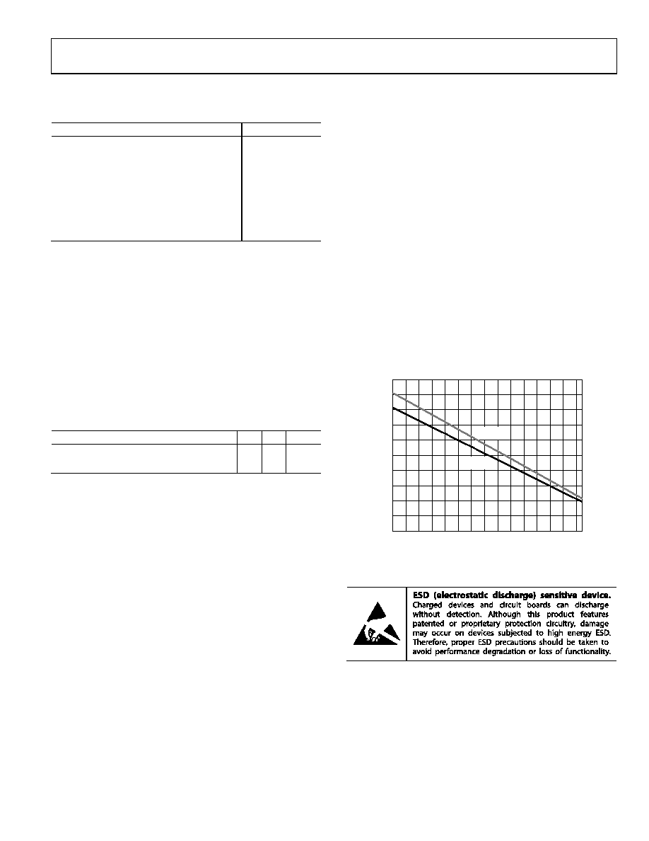
Figure 4 shows the maximum power dissipation vs. the ambient
temperature for the single and dual 8-lead SOIC_N_EP on a
JEDEC standard 4-layer board, with its underside paddle
soldered to a pad that is thermally connected to a PCB plane. θJA
values are approximations.
0
0.5
1.0
1.5
2.0
2.5
3.0
3.5
4.0
5.0
4.5
07037-
003
AMBIENT TEMPERATURE (°C)
MA
XI
MU
M
PO
W
ER
D
ISSI
PA
T
IO
N
(W
)
0
20
40
60
80
100
10
30
50
70
90
–40
–20
–30
–10
ADA4898-2
ADA4898-1
Figure 4. Maximum Power Dissipation vs. Ambient Temperature
ESD CAUTION
相关PDF资料 |
PDF描述 |
|---|---|
| PEC17DGBN | CONN HEADER .100 DUAL R/A 34POS |
| PEC22DGAN | CONN HEADER .100 DUAL R/A 44POS |
| 1761685-6 | CONN HEADER IDC 16POS VERT GOLD |
| PEC31DBBN | CONN HEADER .100 DUAL R/A 62POS |
| OP285GSZ-REEL7 | IC OPAMP GP 9MHZ DUAL PREC 8SOIC |
相关代理商/技术参数 |
参数描述 |
|---|---|
| MCP65R41T-1202E/CHY | 功能描述:校验器 IC Single Push/Pull Comparator 1.2V Ref RoHS:否 制造商:STMicroelectronics 产品: 比较器类型: 通道数量: 输出类型:Push-Pull 电源电压-最大:5.5 V 电源电压-最小:1.1 V 补偿电压(最大值):6 mV 电源电流(最大值):1350 nA 响应时间: 最大工作温度:+ 125 C 安装风格:SMD/SMT 封装 / 箱体:SC-70-5 封装:Reel |
| MCP65R41T-2402E/CHY | 功能描述:校验器 IC Single Push/Pull Comparator 2.4V Ref RoHS:否 制造商:STMicroelectronics 产品: 比较器类型: 通道数量: 输出类型:Push-Pull 电源电压-最大:5.5 V 电源电压-最小:1.1 V 补偿电压(最大值):6 mV 电源电流(最大值):1350 nA 响应时间: 最大工作温度:+ 125 C 安装风格:SMD/SMT 封装 / 箱体:SC-70-5 封装:Reel |
| MCP65R46T-1202E/CHY | 功能描述:校验器 IC Single Open Drain Comparator 1.2V Ref RoHS:否 制造商:STMicroelectronics 产品: 比较器类型: 通道数量: 输出类型:Push-Pull 电源电压-最大:5.5 V 电源电压-最小:1.1 V 补偿电压(最大值):6 mV 电源电流(最大值):1350 nA 响应时间: 最大工作温度:+ 125 C 安装风格:SMD/SMT 封装 / 箱体:SC-70-5 封装:Reel |
| MCP65R46T-2402E/CHY | 功能描述:校验器 IC Single Open Drain Comparator 2.4V Ref RoHS:否 制造商:STMicroelectronics 产品: 比较器类型: 通道数量: 输出类型:Push-Pull 电源电压-最大:5.5 V 电源电压-最小:1.1 V 补偿电压(最大值):6 mV 电源电流(最大值):1350 nA 响应时间: 最大工作温度:+ 125 C 安装风格:SMD/SMT 封装 / 箱体:SC-70-5 封装:Reel |
| MCP660-E/ML | 功能描述:运算放大器 - 运放 Triple 60MHz OP w/CS E temp RoHS:否 制造商:STMicroelectronics 通道数量:4 共模抑制比(最小值):63 dB 输入补偿电压:1 mV 输入偏流(最大值):10 pA 工作电源电压:2.7 V to 5.5 V 安装风格:SMD/SMT 封装 / 箱体:QFN-16 转换速度:0.89 V/us 关闭:No 输出电流:55 mA 最大工作温度:+ 125 C 封装:Reel |
发布紧急采购,3分钟左右您将得到回复。