- 您现在的位置:买卖IC网 > PDF目录182422 > MJD47-1 (ON SEMICONDUCTOR) 1 A, 250 V, NPN, Si, POWER TRANSISTOR PDF资料下载
参数资料
| 型号: | MJD47-1 |
| 厂商: | ON SEMICONDUCTOR |
| 元件分类: | 功率晶体管 |
| 英文描述: | 1 A, 250 V, NPN, Si, POWER TRANSISTOR |
| 封装: | CASE 369-07, 3 PIN |
| 文件页数: | 1/8页 |
| 文件大小: | 0K |
| 代理商: | MJD47-1 |
High Voltage Power Transistors
DPAK For Surface Mount Applications
Designed for line operated audio output amplifier,
SWITCHMODE
t power supply drivers and other switching
applications.
Lead Formed for Surface Mount Applications in Plastic Sleeves (No
Suffix)
Straight Lead Version in Plastic Sleeves (“–1” Suffix)
Lead Formed Version in 16 mm Tape and Reel (“T4” Suffix)
Electrically Similar to Popular TIP47, and TIP50
250 and 400 V (Min) — V
CEO(sus)
1 A Rated Collector Current
MAXIMUM RATINGS
Rating
Symbol
MJD47
MJD50
Unit
Collector–Emitter Voltage
VCEO
250
400
Vdc
Collector–Base Voltage
VCB
350
500
Vdc
Emitter–Base Voltage
VEB
5
Vdc
Collector Current — Continuous
Peak
IC
1
2
Adc
Base Current
IB
0.6
Adc
Total Power Dissipation @ TC = 25_C
Derate above 25
_C
PD
15
0.12
Watts
W/
_C
Total Power Dissipation* @ TA = 25_C
Derate above 25
_C
PD
1.56
0.0125
Watts
W/
_C
Operating and Storage Junction
Temperature Range
TJ, Tstg
–65 to +150
_C
THERMAL CHARACTERISTICS
Characteristic
Symbol
Max
Unit
Thermal Resistance, Junction to Case
RθJC
8.33
_C/W
Thermal Resistance, Junction to Ambient*
RθJA
80
_C/W
Lead Temperature for Soldering Purpose
TL
260
_C
ELECTRICAL CHARACTERISTICS (TC = 25_C unless otherwise noted)
Characteristic
Symbol
Min
Max
Unit
OFF CHARACTERISTICS
Collector–Emitter Sustaining Voltage (1) MJD47
(IC = 30 mAdc, IB = 0)
MJD50
VCEO(sus)
250
400
—
Vdc
Collector Cutoff Current
(VCE = 150 Vdc, IB = 0)
MJD47
(VCE = 300 Vdc, IB = 0)
MJD50
ICEO
—
0.2
mAdc
*When surface mounted on minimum pad sizes recommended.
(continued)
(1) Pulse Test: Pulse Width
v 300 s, Duty Cycle v 2%.
Preferred devices are ON Semiconductor recommended choices for future use and best overall value.
ON Semiconductort
Semiconductor Components Industries, LLC, 2001
November, 2001 – Rev. 4
1
Publication Order Number:
MJD47/D
NPN SILICON
POWER TRANSISTORS
1 AMPERE
250, 400 VOLTS
15 WATTS
MJD47
MJD50
*ON Semiconductor Preferred Device
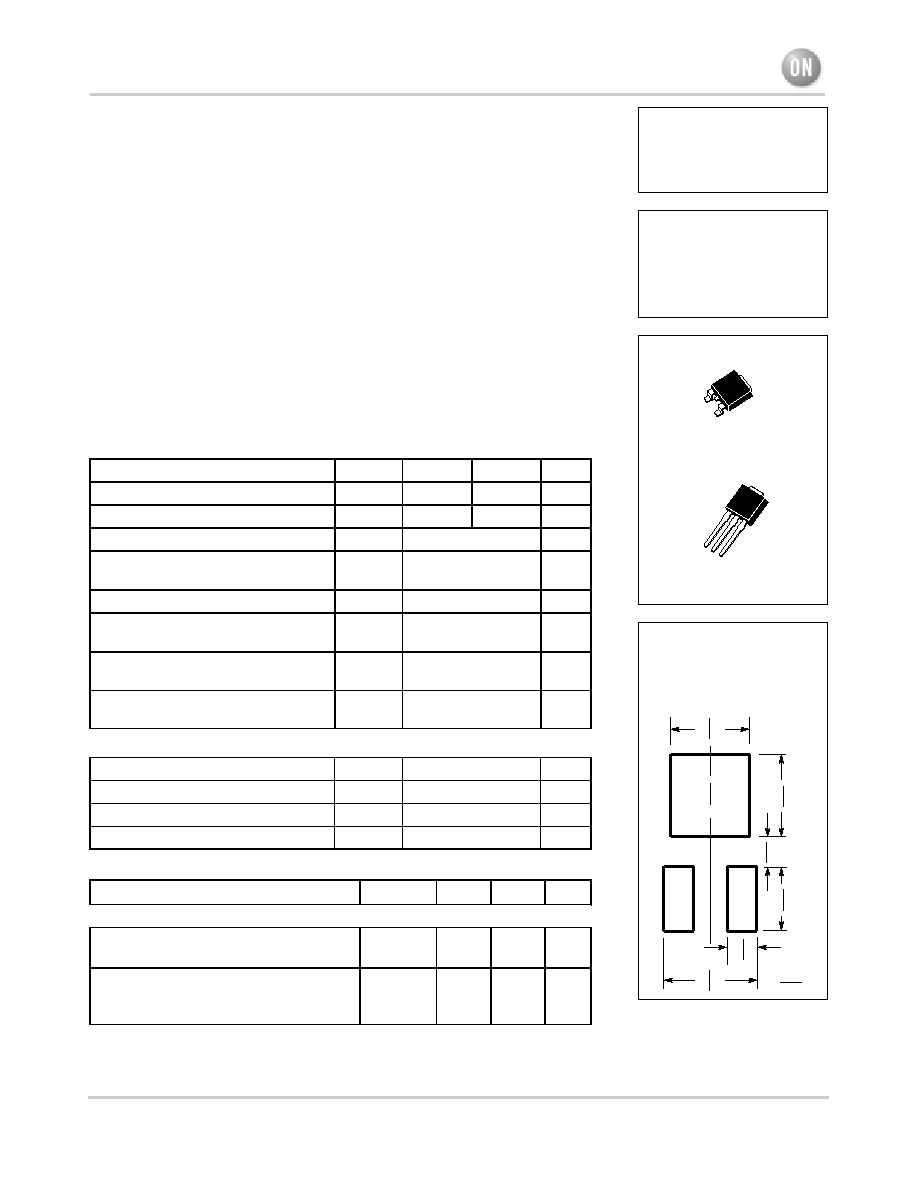
MINIMUM PAD SIZES
RECOMMENDED FOR
SURFACE MOUNTED
APPLICATIONS
CASE 369A–13
CASE 369–07
*
0.243 6.172
0.063 1.6
0.1
18
3.0
0.100 2.54
0.165 4.191
0.190 4.826
inches
mm
相关PDF资料 |
PDF描述 |
|---|---|
| MJD50I | 1 A, 400 V, NPN, Si, POWER TRANSISTOR |
| MJD47I | 1 A, 250 V, NPN, Si, POWER TRANSISTOR |
| MJD50 | 1 A, 400 V, NPN, Si, POWER TRANSISTOR, TO-252 |
| MJDS-G | FEMALE, TELECOM AND DATACOM CONNECTOR, SOLDER, JACK |
| MJDS-LG5-86-2GF5S-30 | 12 CONTACT(S), FEMALE, TELECOM AND DATACOM CONNECTOR, SOLDER, JACK |
相关代理商/技术参数 |
参数描述 |
|---|---|
| MJD474 | 制造商: 功能描述: 制造商:undefined 功能描述: |
| MJD47G | 功能描述:两极晶体管 - BJT 1A 250V 15W NPN RoHS:否 制造商:STMicroelectronics 配置: 晶体管极性:PNP 集电极—基极电压 VCBO: 集电极—发射极最大电压 VCEO:- 40 V 发射极 - 基极电压 VEBO:- 6 V 集电极—射极饱和电压: 最大直流电集电极电流: 增益带宽产品fT: 直流集电极/Base Gain hfe Min:100 A 最大工作温度: 安装风格:SMD/SMT 封装 / 箱体:PowerFLAT 2 x 2 |
| MJD47MJD50 | 制造商:TYSEMI 制造商全称:TY Semiconductor Co., Ltd 功能描述:Load Formed for Surface Mount Application |
| MJD47T4 | 功能描述:两极晶体管 - BJT NPN Hi-Volt Fast Sw RoHS:否 制造商:STMicroelectronics 配置: 晶体管极性:PNP 集电极—基极电压 VCBO: 集电极—发射极最大电压 VCEO:- 40 V 发射极 - 基极电压 VEBO:- 6 V 集电极—射极饱和电压: 最大直流电集电极电流: 增益带宽产品fT: 直流集电极/Base Gain hfe Min:100 A 最大工作温度: 安装风格:SMD/SMT 封装 / 箱体:PowerFLAT 2 x 2 |
| MJD47T4G | 功能描述:两极晶体管 - BJT 1A 250V 15W NPN RoHS:否 制造商:STMicroelectronics 配置: 晶体管极性:PNP 集电极—基极电压 VCBO: 集电极—发射极最大电压 VCEO:- 40 V 发射极 - 基极电压 VEBO:- 6 V 集电极—射极饱和电压: 最大直流电集电极电流: 增益带宽产品fT: 直流集电极/Base Gain hfe Min:100 A 最大工作温度: 安装风格:SMD/SMT 封装 / 箱体:PowerFLAT 2 x 2 |
发布紧急采购,3分钟左右您将得到回复。