- 您现在的位置:买卖IC网 > PDF目录80516 > MPC8560CVT667JC (FREESCALE SEMICONDUCTOR INC) 32-BIT, 667 MHz, RISC PROCESSOR, PBGA783 PDF资料下载
参数资料
| 型号: | MPC8560CVT667JC |
| 厂商: | FREESCALE SEMICONDUCTOR INC |
| 元件分类: | 微控制器/微处理器 |
| 英文描述: | 32-BIT, 667 MHz, RISC PROCESSOR, PBGA783 |
| 封装: | 29 X 29 MM, 3.75 MM HEIGHT, 1 MM PITCH, LEAD FREE, PLASTIC, FCBGA-783 |
| 文件页数: | 18/104页 |
| 文件大小: | 1244K |
| 代理商: | MPC8560CVT667JC |
第1页第2页第3页第4页第5页第6页第7页第8页第9页第10页第11页第12页第13页第14页第15页第16页第17页当前第18页第19页第20页第21页第22页第23页第24页第25页第26页第27页第28页第29页第30页第31页第32页第33页第34页第35页第36页第37页第38页第39页第40页第41页第42页第43页第44页第45页第46页第47页第48页第49页第50页第51页第52页第53页第54页第55页第56页第57页第58页第59页第60页第61页第62页第63页第64页第65页第66页第67页第68页第69页第70页第71页第72页第73页第74页第75页第76页第77页第78页第79页第80页第81页第82页第83页第84页第85页第86页第87页第88页第89页第90页第91页第92页第93页第94页第95页第96页第97页第98页第99页第100页第101页第102页第103页第104页
MPC8560 Integrated Processor Hardware Specifications, Rev. 5
20
Freescale Semiconductor
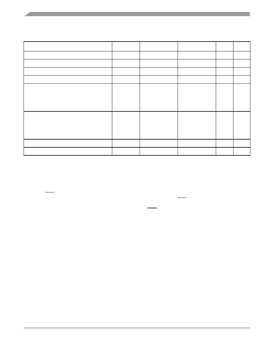
DDR SDRAM
MCK[n] duty cycle
tMCKH/tMCK
45
55
%
8
ADDR/CMD output valid
tDDKHOV
—3
ns
4, 9
ADDR/CMD output invalid
tDDKHOX
1—
ns
4, 9
Write CMD to first MDQS capture edge
tDDSHMH
tMCK + 1.5
tMCK + 4.0
ns
5
MDQ/MECC/MDM output setup with respect to
MDQS
333 MHz
266 MHz
200 MHz
tDDKHDS,
tDDKLDS
900
1100
1200
—ps
6, 9
MDQ/MECC/MDM output hold with respect to
MDQS
333 MHz
266 MHz
200 MHz
tDDKHDX,
tDDKLDX
900
1100
1200
—ps
6, 9
MDQS preamble start
tDDSHMP
0.75
× tMCK + 1.5
0.75
× tMCK + 4.0
ns
7, 8
MDQS epilogue end
tDDSHME
1.5
4.0
ns
7, 8
Notes:
1. The symbols used for timing specifications follow the pattern of t(first two letters of functional block)(signal)(state) (reference)(state) for
inputs and t(first two letters of functional block)(reference)(state)(signal)(state) for outputs. Output hold time can be read as DDR timing
(DD) from the rising or falling edge of the reference clock (KH or KL) until the output went invalid (OX or DX). For example,
tDDKHOV symbolizes DDR timing (DD) for the time tMCK memory clock reference (K) goes from the high (H) state until outputs
(O) are valid (V) or output valid time. Also, tDDKLDX symbolizes DDR timing (DD) for the time tMCK memory clock reference
(K) goes low (L) until data outputs (D) are invalid (X) or data output hold time.
2. All MCK/MCK referenced measurements are made from the crossing of the two signals ±0.1 V.
3. Maximum possible clock skew between a clock MCK[n] and its relative inverse clock MCK[n], or between a clock MCK[n] and
a relative clock MCK[m] or MSYNC_OUT. Skew measured between complementary signals at GVDD/2.
4. ADDR/CMD includes all DDR SDRAM output signals except MCK/MCK and MDQ/MECC/MDM/MDQS.
5. Note that tDDSHMH follows the symbol conventions described in note 1. For example, tDDSHMH describes the DDR timing (DD)
from the rising edge of the MSYNC_IN clock (SH) until the MDQS signal is valid (MH). tDDSHMH can be modified through
control of the DQSS override bits in the TIMING_CFG_2 register. These controls allow the relationship between the
synchronous clock control timing and the source-synchronous DQS domain to be modified by the user. For best turnaround
times, these may need to be set to delay tDDSHMH an additional 0.25tMCK. This will also affect tDDSHMP and tDDSHME
accordingly. See the MPC8560 PowerQUICC III Integrated Communications Processor Reference Manual for a description
and understanding of the timing modifications enabled by use of these bits.
6. Determined by maximum possible skew between a data strobe (MDQS) and any corresponding bit of data (MDQ), ECC
(MECC), or data mask (MDM). The data strobe should be centered inside of the data eye at the pins of the device.
7. All outputs are referenced to the rising edge of MSYNC_IN (S) at the pins of the device. Note that tDDSHMP follows the symbol
conventions described in note 1. For example, tDDSHMP describes the DDR timing (DD) from the rising edge of the MSYNC_IN
clock (SH) for the duration of the MDQS signal precharge period (MP).
8. Guaranteed by design.
9. Guaranteed by characterization.
Table 16. DDR SDRAM Output AC Timing Specifications–DLL Mode (continued)
At recommended operating conditions with GVDD of 2.5 V ± 5%.
Parameter
Symbol 1
Min
Max
Unit
Notes
相关PDF资料 |
PDF描述 |
|---|---|
| M926-02I622.0800 | 622.08 MHz, OTHER CLOCK GENERATOR, CQCC36 |
| M928-02-700.0000 | 700 MHz, OTHER CLOCK GENERATOR, CQCC36 |
| MK1411SLF | 35.46896 MHz, VIDEO CLOCK GENERATOR, PDSO8 |
| MK1726-01SLF | 32 MHz, OTHER CLOCK GENERATOR, PDSO8 |
| MK1726-02AS | 64 MHz, OTHER CLOCK GENERATOR, PDSO8 |
相关代理商/技术参数 |
参数描述 |
|---|---|
| MPC8560CVT667LB | 功能描述:微处理器 - MPU PQ 3 8560 Dracom RoHS:否 制造商:Atmel 处理器系列:SAMA5D31 核心:ARM Cortex A5 数据总线宽度:32 bit 最大时钟频率:536 MHz 程序存储器大小:32 KB 数据 RAM 大小:128 KB 接口类型:CAN, Ethernet, LIN, SPI,TWI, UART, USB 工作电源电压:1.8 V to 3.3 V 最大工作温度:+ 85 C 安装风格:SMD/SMT 封装 / 箱体:FBGA-324 |
| MPC8560PX667LB | 功能描述:微处理器 - MPU PQ 3 8560-DRACOM RoHS:否 制造商:Atmel 处理器系列:SAMA5D31 核心:ARM Cortex A5 数据总线宽度:32 bit 最大时钟频率:536 MHz 程序存储器大小:32 KB 数据 RAM 大小:128 KB 接口类型:CAN, Ethernet, LIN, SPI,TWI, UART, USB 工作电源电压:1.8 V to 3.3 V 最大工作温度:+ 85 C 安装风格:SMD/SMT 封装 / 箱体:FBGA-324 |
| MPC8560PX667LC | 功能描述:微处理器 - MPU PQ 3 8560-DRACOM RoHS:否 制造商:Atmel 处理器系列:SAMA5D31 核心:ARM Cortex A5 数据总线宽度:32 bit 最大时钟频率:536 MHz 程序存储器大小:32 KB 数据 RAM 大小:128 KB 接口类型:CAN, Ethernet, LIN, SPI,TWI, UART, USB 工作电源电压:1.8 V to 3.3 V 最大工作温度:+ 85 C 安装风格:SMD/SMT 封装 / 箱体:FBGA-324 |
| MPC8560PX833LB | 功能描述:微处理器 - MPU PQ 3 8560-DRACOM RoHS:否 制造商:Atmel 处理器系列:SAMA5D31 核心:ARM Cortex A5 数据总线宽度:32 bit 最大时钟频率:536 MHz 程序存储器大小:32 KB 数据 RAM 大小:128 KB 接口类型:CAN, Ethernet, LIN, SPI,TWI, UART, USB 工作电源电压:1.8 V to 3.3 V 最大工作温度:+ 85 C 安装风格:SMD/SMT 封装 / 箱体:FBGA-324 |
| MPC8560PX833LC | 功能描述:微处理器 - MPU PQ 3 8560-DRACOM RoHS:否 制造商:Atmel 处理器系列:SAMA5D31 核心:ARM Cortex A5 数据总线宽度:32 bit 最大时钟频率:536 MHz 程序存储器大小:32 KB 数据 RAM 大小:128 KB 接口类型:CAN, Ethernet, LIN, SPI,TWI, UART, USB 工作电源电压:1.8 V to 3.3 V 最大工作温度:+ 85 C 安装风格:SMD/SMT 封装 / 箱体:FBGA-324 |
发布紧急采购,3分钟左右您将得到回复。