- 您现在的位置:买卖IC网 > PDF目录18823 > ZNBG4001Q16TC (Diodes Inc)IC GENERATOR 4BIAS 2.0V 16-QSOP PDF资料下载
参数资料
| 型号: | ZNBG4001Q16TC |
| 厂商: | Diodes Inc |
| 文件页数: | 6/10页 |
| 文件大小: | 0K |
| 描述: | IC GENERATOR 4BIAS 2.0V 16-QSOP |
| 标准包装: | 2,500 |
| 功能: | 偏压控制器 |
| RF 型: | LNBs,PMR |
| 封装/外壳: | 16-SSOP(0.154",3.90mm 宽) |
| 包装: | 带卷 (TR) |
�� �
�
�ZNBG4000� ZNBG4001�
�ZNBG6000� ZNBG6001�
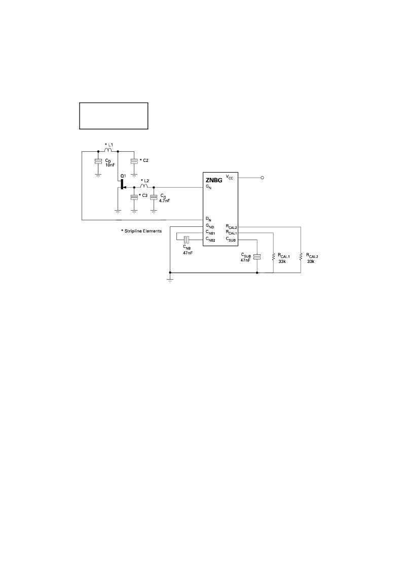
�TYPICAL� APPLICATION� CIRCUIT�
�APPLICATIONS� INFORMATION�
�The� above� is� a� partial� application� circuit� for� the� ZNBG� series� showing� all� external� components�
�required� for� appropriate� biasing.� The� bias� circuits� are� unconditionally� stable� over� the� full�
�temperature� range� with� the� associated� FETs� and� gate� and� drain� capacitors� in� circuit.�
�Capacitors� C� D� and� C� G� ensure� that� residual� power� supply� and� substrate� generator� noise� is� not�
�allowed� to� affect� other� external� circuits� which� may� be� sensitive� to� RF� interference.� They� also�
�serve� to� suppress� any� potential� RF� feedthrough� between� stages� via� the� ZNBG� device.� These�
�capacitors� are� required� for� all� stages� used.� Values� of� 10nF� and� 4.7nF� respectively� are�
�recommended� however� this� is� design� dependent� and� any� value� between� 1nF� and� 100nF� could�
�be� used.�
�The� capacitors� C� NB� and� C� SUB� are� an� integral� part� of� the� ZNBGs� negative� supply� generator.� The�
�negative� bias� voltage� is� generated� on-chip� using� an� internal� oscillator.� The� required� value� of�
�capacitors� C� NB� and� C� SUB� is� 47nF.� This� generator� produces� a� low� current� supply� of� approximately�
�-3� volts.� Although� this� generator� is� intended� purely� to� bias� the� external� FETs,� it� can� be� used� to�
�power� other� external� circuits� via� the� C� SUB� pin.�
�Resistors� R� CAL1/2� sets� the� drain� current� at� which� all� external� FETs� are� operated.� Both� ZNBG� devices�
�have� the� facility� to� program� different� drain� currents� into� selected� FETs.� Two� R� CAL� inputs� are�
�provided.� For� the� ZNBG4000,� resistor� R� CAL1� sets� the� drain� current� of� FETs� 1� and� 2,� resistor� R� CAL2�
�sets� the� drain� current� of� FETs� 3� and� 4.� For� the� ZNBG6000,� resistor� R� CAL1� sets� the� drain� current�
�of� FETs� 1� and� 4,� resistor� R� CAL2� sets� the� drain� current� of� FETs� 2,� 3,� 5� and� 6.� If� the� same� drain� current�
�is� required� for� all� FETs� on� either� device� then� pins� R� CAL1� and� R� CAL2� can� be� wired� together� and�
�shunted� to� ground� by� a� single� calibration� resistor� of� half� normal� value.�
�If� any� bias� control� circuit� is� not� required,� its� related� drain� and� gate� connections� may� be� left� open�
�circuit� without� affecting� the� operation� of� the� remaining� bias� circuits.� If� all� FETs� associated� with�
�a� current� setting� resistor� are� omitted,� the� particular� R� CAL� should� still� be� included.� The� supply�
�current� can� be� reduced,� if� required,� by� using� a� high� value� R� CAL� resistor� (e.g.� 470k).�
�4-142�
�相关PDF资料 |
PDF描述 |
|---|---|
| T7H8067504DN | SCR PHASE CTRL MOD 600V 750A |
| CM421290 | SCR MOD PWR-BLK 1200V 90A |
| ZLNB2009Q20TC | MUX DUAL DUAL H/V TONE SW 20QSOP |
| KC7050P155.520L30E00 | OSC 155.52MHZ 3.3V LVDS SMD |
| KC7050P155.520P30E00 | OSC 155.52MHZ 3.3V PECL SMD |
相关代理商/技术参数 |
参数描述 |
|---|---|
| MPC9600AER2 | 功能描述:时钟缓冲器 RoHS:否 制造商:Texas Instruments 输出端数量:5 最大输入频率:40 MHz 传播延迟(最大值): 电源电压-最大:3.45 V 电源电压-最小:2.375 V 最大功率耗散: 最大工作温度:+ 85 C 最小工作温度:- 40 C 封装 / 箱体:LLP-24 封装:Reel |
| MPC9600FA | 功能描述:IC CLOCK DRVR PLL LV 1:21 48LQFP RoHS:否 类别:集成电路 (IC) >> 时钟/计时 - 时钟发生器,PLL,频率合成器 系列:- 标准包装:39 系列:- 类型:* PLL:带旁路 输入:时钟 输出:时钟 电路数:1 比率 - 输入:输出:1:10 差分 - 输入:输出:是/是 频率 - 最大:170MHz 除法器/乘法器:无/无 电源电压:2.375 V ~ 3.465 V 工作温度:0°C ~ 70°C 安装类型:* 封装/外壳:* 供应商设备封装:* 包装:* |
| MPC9608 | 制造商:MOTOROLA 制造商全称:Motorola, Inc 功能描述:1:10 LVCMOS Zero Delay Clock Buffer |
| MPC9608AC | 功能描述:时钟缓冲器 RoHS:否 制造商:Texas Instruments 输出端数量:5 最大输入频率:40 MHz 传播延迟(最大值): 电源电压-最大:3.45 V 电源电压-最小:2.375 V 最大功率耗散: 最大工作温度:+ 85 C 最小工作温度:- 40 C 封装 / 箱体:LLP-24 封装:Reel |
| MPC9608ACR2 | 功能描述:时钟缓冲器 RoHS:否 制造商:Texas Instruments 输出端数量:5 最大输入频率:40 MHz 传播延迟(最大值): 电源电压-最大:3.45 V 电源电压-最小:2.375 V 最大功率耗散: 最大工作温度:+ 85 C 最小工作温度:- 40 C 封装 / 箱体:LLP-24 封装:Reel |
发布紧急采购,3分钟左右您将得到回复。