- 您现在的位置:买卖IC网 > PDF目录16752 > NCN8025AMNGEVB (ON Semiconductor)BOARD EVAL SMART CARD INTERFACE PDF资料下载
参数资料
| 型号: | NCN8025AMNGEVB |
| 厂商: | ON Semiconductor |
| 文件页数: | 10/15页 |
| 文件大小: | 0K |
| 描述: | BOARD EVAL SMART CARD INTERFACE |
| 设计资源: | NCN8025AMNGEVB Test Procedure NCN8025AMNGEVB Gerber Zip NCN8025AMNGEVB Bill of Materials NCN8025AMNGEVB Schematic |
| 标准包装: | 1 |
| 主要目的: | 接口,智能卡 |
| 嵌入式: | 否 |
| 已用 IC / 零件: | NCN8025A |
| 已供物品: | 板 |
| 其它名称: | NCN8025AMNGEVB-ND NCN8025AMNGEVBOS |
NCN8025 / NCN8025A
http://onsemi.com
4
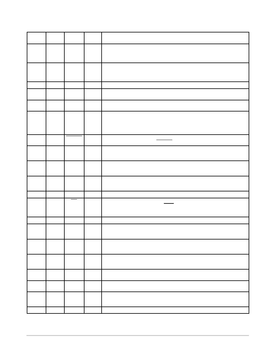
PIN FUNCTION AND DESCRIPTION
Pin
(QFN24)
Description
Type
Name
Pin
(QFN16)
6
CAUX2
Input/
Output
This pin handles the connection to the chip card’s serial auxiliary AUX2 I/O pin (C8). A
bidirectional level translator adapts the serial I/O signal between the card and the micro
controller. A 11 kW (typical) pull up resistor to CVCC provides a High impedance state for
the smart card C8 pin.
7
CAUX1
Input/
Output
This pin handles the connection to the chip card’s serial auxiliary AUX1 I/O pin (C4). A
bidirectional level translator adapts the serial I/O signal between the card and the micro
controller. A 11 kW (typical) pull up resistor to CVCC provides a High impedance state for
the smart card C4 pin.
8
GND
Ground
Card Ground
9
5
CCLK
Output
This pin is connected to the CLOCK card connector’s pin (Chip card’s pin C3). The Clock
signal comes from the CLKIN input through clock dividers and level shifter.
10
6
CRST
Output
This pin is connected to the chip card’s RESET pin (C2) through the card connector. A
level translator adapts the external Reset (RSTIN) signal to the smart card.
11
7
CVCC
Power
Output
This pin is connected to the smart card power supply pin (C1). An internal low dropout
regulator is programmable using the pins VSEL0 and VSEL1 to supply either 5 V or 3 V
or 1.8 V output voltage. An external distributed ceramic capacitor ranging from 80 nF to
1.2 mF recommended must be connected across CVCC and CGND. This set of capacitor
(if distributed) must be low ESR (< 100 mW).
12
8
CMDVCC
Input
Command VCC pin. Activation sequence Enable/Disable pin (active Low). The activation
sequence is enabled by toggling CMDVCC High to Low and when a card is present.
13
PORADJ
Input
Poweron reset threshold adjustment input pin for changing the reset threshold (VDD
UVLO threshold) thanks to an external resistor power divider. Needs to be connected to
ground when unused.
14
9
RSTIN
Input
This Reset input connected to the host and referred to VDD (microcontroller side), is
connected to the smart card Reset pin through the internal level shifter which translates
the level according to the CVCC programmed value.
15
10
VDD
Power
input
This pin is connected to the system controller power supply. It configures the level shifter
input stage to accept the signals coming from the controller. A 0.1 mF decoupling
capacitor shall be used. When VDD is below 2.30 V typical the card pins are disabled.
16
GND
Ground
17
11
INT
Output
The interrupt request is activated LOW on this pin. This is enabled when a card is present
and the card presence is detected by PRES or PRES pins. Similarly an interrupt is
generated when CVCC is overloaded. Inverter output (An opendrain output configuration
with 50 kW pullup resistor is available under request (metal change)).
18
12
CLKIN
Input
Clock Input for External Clock
19
13
I/Ouc
Input /
Output
This pin is connected to an external microcontroller. A bidirectional level translator
adapts the serial I/O signal between the smart card and the external controller. A builtin
constant 11 kW (typical) resistor provides a high impedance state.
20
AUX1uc
Input /
Output
This pin is connected to an external microcontroller. A bidirectional level translator
adapts the serial C4 signal between the smart card and the external controller. A builtin
constant 11 kW (typical) resistor provides a high impedance state.
21
AUX2uc
Input /
Output
This pin is connected to an external microcontroller. A bidirectional level translator
adapts the serial C8 signal between the smart card and the external controller. A builtin
constant 11 kW (typical) resistor provides a high impedance state.
22
14
CLKDIV1
Input
This pin coupled with CLKDIV2 is used to program the clock frequency division ratio
(Table 2).
23
15
CLKDIV2
Input
This pin coupled with CLKDIV1 is used to program the clock frequency division ratio
(Table 2).
24
16
VSEL1
Input
Allows selecting card VCC power supply voltage.
VSEL0 = Low: CVCC = 5 V when VSEL1 = High or 3 V when VSEL1 = Low.
VSEL0 = High: CVCC = 1.8 V when VSEL1 = High or 3 V when VSEL1 = Low.
25
17
GND
Ground
Regulator Power Supply Ground
NOTE: All information below refers to QFN24 pin numbering unless otherwise noted. This information can be transposed to
the QFN16 package according to the above “PIN FUNCTION AND DESCRIPTION” Table.
相关PDF资料 |
PDF描述 |
|---|---|
| RCC18DRTI-S13 | CONN EDGECARD 36POS .100 EXTEND |
| GBM25DTAI-S189 | CONN EDGECARD 50POS R/A .156 SLD |
| 0982660997 | CBL 29POS 0.5MM JMPR TYPE A 6" |
| H3AAS-3406M | IDC CABLE - HSC34S/AE34M/HSC34S |
| 0982660064 | CBL 6POS 0.5MM JMPR TYPE D 7" |
相关代理商/技术参数 |
参数描述 |
|---|---|
| NCN8025AMNTXG | 功能描述:接口 - 专用 SMART CARD IC RoHS:否 制造商:Texas Instruments 产品类型:1080p60 Image Sensor Receiver 工作电源电压:1.8 V 电源电流:89 mA 最大功率耗散: 最大工作温度:+ 85 C 安装风格:SMD/SMT 封装 / 箱体:BGA-59 |
| NCN8025MTTBG | 功能描述:接口 - 专用 SMART CARD IC RoHS:否 制造商:Texas Instruments 产品类型:1080p60 Image Sensor Receiver 工作电源电压:1.8 V 电源电流:89 mA 最大功率耗散: 最大工作温度:+ 85 C 安装风格:SMD/SMT 封装 / 箱体:BGA-59 |
| NCN8026A | 制造商:ONSEMI 制造商全称:ON Semiconductor 功能描述:Compact Low Power Smart Card Interface IC |
| NCN8026AMNGEVB | 制造商:ON Semiconductor 功能描述:NCN8026A QFN24L EVAL BD - Bulk 制造商:ON Semiconductor 功能描述:Interface Development Tools NCN8026A QFN24L Smart Card IF |
| NCN8026AMNTXG | 制造商:ON Semiconductor 功能描述:SMART CARD IC IN QFN 24L - Tape and Reel |
发布紧急采购,3分钟左右您将得到回复。