- 您现在的位置:买卖IC网 > PDF目录224624 > OR2C06A-3S256I (Electronic Theatre Controls, Inc.) Field-Programmable Gate Arrays PDF资料下载
参数资料
| 型号: | OR2C06A-3S256I |
| 厂商: | Electronic Theatre Controls, Inc. |
| 元件分类: | FPGA |
| 英文描述: | Field-Programmable Gate Arrays |
| 中文描述: | 现场可编程门阵列 |
| 文件页数: | 149/192页 |
| 文件大小: | 3148K |
| 代理商: | OR2C06A-3S256I |
第1页第2页第3页第4页第5页第6页第7页第8页第9页第10页第11页第12页第13页第14页第15页第16页第17页第18页第19页第20页第21页第22页第23页第24页第25页第26页第27页第28页第29页第30页第31页第32页第33页第34页第35页第36页第37页第38页第39页第40页第41页第42页第43页第44页第45页第46页第47页第48页第49页第50页第51页第52页第53页第54页第55页第56页第57页第58页第59页第60页第61页第62页第63页第64页第65页第66页第67页第68页第69页第70页第71页第72页第73页第74页第75页第76页第77页第78页第79页第80页第81页第82页第83页第84页第85页第86页第87页第88页第89页第90页第91页第92页第93页第94页第95页第96页第97页第98页第99页第100页第101页第102页第103页第104页第105页第106页第107页第108页第109页第110页第111页第112页第113页第114页第115页第116页第117页第118页第119页第120页第121页第122页第123页第124页第125页第126页第127页第128页第129页第130页第131页第132页第133页第134页第135页第136页第137页第138页第139页第140页第141页第142页第143页第144页第145页第146页第147页第148页当前第149页第150页第151页第152页第153页第154页第155页第156页第157页第158页第159页第160页第161页第162页第163页第164页第165页第166页第167页第168页第169页第170页第171页第172页第173页第174页第175页第176页第177页第178页第179页第180页第181页第182页第183页第184页第185页第186页第187页第188页第189页第190页第191页第192页
Data Sheet
ORCA Series 2 FPGAs
June 1999
6
Lucent Technologies Inc.
Programmable Logic Cells (continued))
Key: C = controlled by configuration RAM.
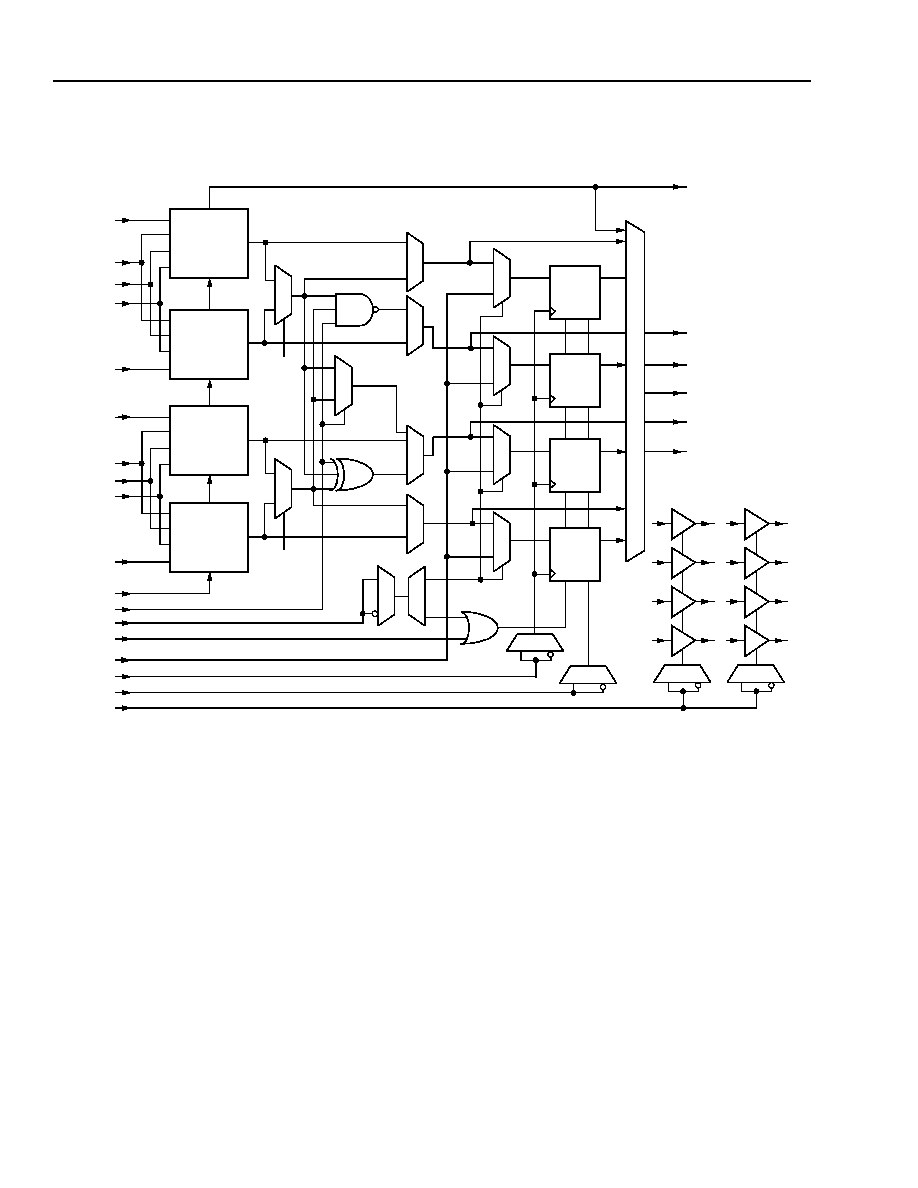
Figure 3. Simplified PFU Diagram
5-4573(F)
A4
A3
A2
A1
A4
A3
A2
A1
QLUT3
A0
CARRY
A3
A2
A1
A0
QLUT2
B4
B3
B2
B1
B4
B3
B2
B1
QLUT1
B0
CARRY
B3
B2
B1
B0
QLUT0
CIN
C0
LSR
GSR
WD[3:0]
CK
CKEN
TRI
PFU_XOR
B4
A4
PFU_NAND
PFU_MUX
C
WD3
WD2
WD1
WD0
C
T
REG3
SR
EN
REG2
SR
EN
REG1
SR
EN
REG0
SR
EN
O4
O3
O2
O1
O0
F3
C
COUT
F2
F1
F0
D0
D1
D2
D3
Q0
Q1
Q2
Q3
C
T
C
views of the ports in the PFU, respectively. The ports
are referenced with a two- to four-character suffix to a
PFU’s location. As mentioned, there are two 5-bit input
data buses (A[4:0] and B[4:0]) to the LUT, one 4-bit
input data bus (WD[3:0]) to the latches/FFs, and an
output data bus (O[4:0]).
Figure 3 shows the four latches/FFs (REG[3:0]) and the
64-bit look-up table (QLUT[3:0]) in the PFU. The PFU
does combinatorial logic in the LUT and sequential
logic in the latches/FFs. The LUT is static random
access memory (SRAM) and can be used for read/
write or read-only memory. The eight 3-state buffers
found in each PLC are also shown, although they actu-
ally reside external to the PFU.
Each latch/FF can accept data from the LUT. Alterna-
tively, the latches/FFs can accept direct data from
WD[3:0], eliminating the LUT delay if no combinatorial
function is needed. The LUT outputs can bypass the
latches/FFs, which reduces the delay out of the PFU. It
is possible to use the LUT and latches/FFs more or
less independently. For example, the latches/FFs can
be used as a 4-bit shift register, and the LUT can be
used to detect when a register has a particular pattern
in it.
相关PDF资料 |
PDF描述 |
|---|---|
| OR2C06A-3S84 | Field-Programmable Gate Arrays |
| OR2C06A-3S84I | Field-Programmable Gate Arrays |
| OR2C06A-3T240 | Field-Programmable Gate Arrays |
| OR2C06A-4M208I | Field-Programmable Gate Arrays |
| OR2C06A-4M240 | Field-Programmable Gate Arrays |
相关代理商/技术参数 |
参数描述 |
|---|---|
| OR2C06A-3S84 | 制造商:未知厂家 制造商全称:未知厂家 功能描述:Field-Programmable Gate Arrays |
| OR2C06A-3S84I | 制造商:未知厂家 制造商全称:未知厂家 功能描述:Field-Programmable Gate Arrays |
| OR2C06A-3T100 | 制造商:未知厂家 制造商全称:未知厂家 功能描述:Field-Programmable Gate Arrays |
| OR2C06A3T100DB | 制造商:ORCA 功能描述:New |
| OR2C06A-3T100I | 制造商:未知厂家 制造商全称:未知厂家 功能描述:Field-Programmable Gate Arrays |
发布紧急采购,3分钟左右您将得到回复。