- 您现在的位置:买卖IC网 > PDF目录224624 > OR2C06A-3S256I (Electronic Theatre Controls, Inc.) Field-Programmable Gate Arrays PDF资料下载
参数资料
| 型号: | OR2C06A-3S256I |
| 厂商: | Electronic Theatre Controls, Inc. |
| 元件分类: | FPGA |
| 英文描述: | Field-Programmable Gate Arrays |
| 中文描述: | 现场可编程门阵列 |
| 文件页数: | 54/192页 |
| 文件大小: | 3148K |
| 代理商: | OR2C06A-3S256I |
第1页第2页第3页第4页第5页第6页第7页第8页第9页第10页第11页第12页第13页第14页第15页第16页第17页第18页第19页第20页第21页第22页第23页第24页第25页第26页第27页第28页第29页第30页第31页第32页第33页第34页第35页第36页第37页第38页第39页第40页第41页第42页第43页第44页第45页第46页第47页第48页第49页第50页第51页第52页第53页当前第54页第55页第56页第57页第58页第59页第60页第61页第62页第63页第64页第65页第66页第67页第68页第69页第70页第71页第72页第73页第74页第75页第76页第77页第78页第79页第80页第81页第82页第83页第84页第85页第86页第87页第88页第89页第90页第91页第92页第93页第94页第95页第96页第97页第98页第99页第100页第101页第102页第103页第104页第105页第106页第107页第108页第109页第110页第111页第112页第113页第114页第115页第116页第117页第118页第119页第120页第121页第122页第123页第124页第125页第126页第127页第128页第129页第130页第131页第132页第133页第134页第135页第136页第137页第138页第139页第140页第141页第142页第143页第144页第145页第146页第147页第148页第149页第150页第151页第152页第153页第154页第155页第156页第157页第158页第159页第160页第161页第162页第163页第164页第165页第166页第167页第168页第169页第170页第171页第172页第173页第174页第175页第176页第177页第178页第179页第180页第181页第182页第183页第184页第185页第186页第187页第188页第189页第190页第191页第192页
Data Sheet
June 1999
ORCA Series 2 FPGAs
Lucent Technologies Inc.
147
Timing Characteristics (continued)
Note: Speed grades of -5, -6, and -7 are for OR2TxxA devices only.
5-4622(F).r2.a
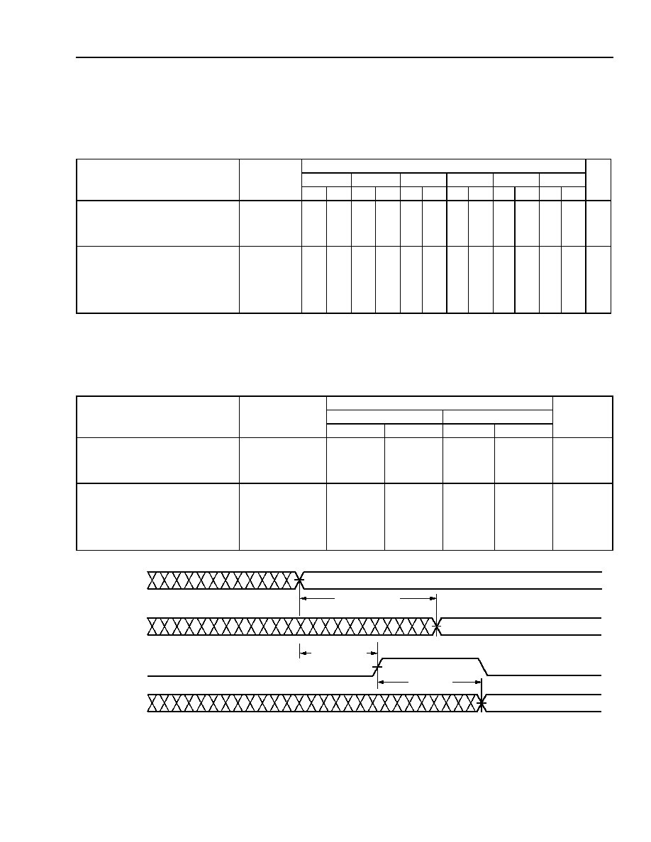
Figure 61. Synchronous Memory Read Cycle
Table 40A. OR2CxxA and OR2TxxA Synchronous Memory Read Characteristics (SSPM and SDPM Modes)
OR2CxxA Commercial: VDD = 5.0 V ± 5%, 0 °C
≤ TA ≤ 70 °C; OR2CxxA Industrial: VDD = 5.0 V ± 10%, –40 °C ≤ TA ≤ +85 °C.
OR2TxxA Commercial: VDD = 3.0 V to 3.6 V, 0 °C
≤ TA ≤ 70 °C; OR2TxxA Industrial: VDD = 3.0 V to 3.6 V, –40 °C ≤ TA ≤
+85 °C.
Parameter
Symbol
Speed
Unit
-2
-3
-4
-5
-6
-7
Min
Max
Min
Max Min Max Min Max Min Max Min Max
Read Operation (TJ = 85 °C, VDD = min):
Read Cycle Time
Data Valid After Address
(A[3:0], B[3:0] to F[3:0])
TRC
MEMS*_ADEL
5.1
—
4.0
3.6
—
2.8
2.7
—
2.1
2.4
—
1.7
2.3
—
1.4
2.0
—
1.1
ns
Read Operation, Clocking Data Into
Latch/FF (TJ = 85 °C, VDD = min):
Address to Clock Setup Time
(A[3:0], B[3:0] to CK)
Clock to PFU Output—Register
(CK to Q[3:0])
MEMS*_ASET
REG_DEL
2.4
—
2.4
1.8
—
2.0
1.2
—
1.9
1.1
—
1.5
1.0
—
1.3
0.9
—
1.0
ns
Table 40B. OR2TxxB Synchronous Memory Read Characteristics (SSPM and SDPM Modes)
OR2TxxB Commercial: VDD = 3.0 V to 3.6 V, 0 °C
≤ TA ≤ 70 °C; OR2TxxB Industrial: VDD = 3.0 V to 3.6 V, –40 °C ≤ TA ≤
+85 °C.
Parameter
Symbol
Speed
Unit
-7
-8
Min
Max
Min
Max
Read Operation (TJ = 85 °C, VDD = min):
Read Cycle Time
Data Valid After Address
(A[3:0], B[3:0] to F[3:0])
TRC
MEMS*_ADEL
1.9
—
1.8
—
1.4
ns
Read Operation, Clocking Data into
Latch/FF (TJ = 85 °C, VDD = Min):
Address to Clock Setup Time
(A[3:0], B[3:0] to CK)
Clock to PFU Output—Register
(CK to Q[3:0])
MEMS*_ASET
REG_DEL
0.9
—
1.0
0.8
—
1.0
ns
A[3:0], B[3:0]
F[3:0]
CK
Q[3:0]
MEM*_ADEL
REG_DEL
MEM*_ASET
相关PDF资料 |
PDF描述 |
|---|---|
| OR2C06A-3S84 | Field-Programmable Gate Arrays |
| OR2C06A-3S84I | Field-Programmable Gate Arrays |
| OR2C06A-3T240 | Field-Programmable Gate Arrays |
| OR2C06A-4M208I | Field-Programmable Gate Arrays |
| OR2C06A-4M240 | Field-Programmable Gate Arrays |
相关代理商/技术参数 |
参数描述 |
|---|---|
| OR2C06A-3S84 | 制造商:未知厂家 制造商全称:未知厂家 功能描述:Field-Programmable Gate Arrays |
| OR2C06A-3S84I | 制造商:未知厂家 制造商全称:未知厂家 功能描述:Field-Programmable Gate Arrays |
| OR2C06A-3T100 | 制造商:未知厂家 制造商全称:未知厂家 功能描述:Field-Programmable Gate Arrays |
| OR2C06A3T100DB | 制造商:ORCA 功能描述:New |
| OR2C06A-3T100I | 制造商:未知厂家 制造商全称:未知厂家 功能描述:Field-Programmable Gate Arrays |
发布紧急采购,3分钟左右您将得到回复。