- 您现在的位置:买卖IC网 > PDF目录299575 > OR3T1257PS208-DB (LATTICE SEMICONDUCTOR CORP) FPGA, 784 CLBS, 186000 GATES, PQFP208 PDF资料下载
参数资料
| 型号: | OR3T1257PS208-DB |
| 厂商: | LATTICE SEMICONDUCTOR CORP |
| 元件分类: | FPGA |
| 英文描述: | FPGA, 784 CLBS, 186000 GATES, PQFP208 |
| 封装: | PLASTIC, SQFP2-208 |
| 文件页数: | 10/203页 |
| 文件大小: | 1368K |
| 代理商: | OR3T1257PS208-DB |
第1页第2页第3页第4页第5页第6页第7页第8页第9页当前第10页第11页第12页第13页第14页第15页第16页第17页第18页第19页第20页第21页第22页第23页第24页第25页第26页第27页第28页第29页第30页第31页第32页第33页第34页第35页第36页第37页第38页第39页第40页第41页第42页第43页第44页第45页第46页第47页第48页第49页第50页第51页第52页第53页第54页第55页第56页第57页第58页第59页第60页第61页第62页第63页第64页第65页第66页第67页第68页第69页第70页第71页第72页第73页第74页第75页第76页第77页第78页第79页第80页第81页第82页第83页第84页第85页第86页第87页第88页第89页第90页第91页第92页第93页第94页第95页第96页第97页第98页第99页第100页第101页第102页第103页第104页第105页第106页第107页第108页第109页第110页第111页第112页第113页第114页第115页第116页第117页第118页第119页第120页第121页第122页第123页第124页第125页第126页第127页第128页第129页第130页第131页第132页第133页第134页第135页第136页第137页第138页第139页第140页第141页第142页第143页第144页第145页第146页第147页第148页第149页第150页第151页第152页第153页第154页第155页第156页第157页第158页第159页第160页第161页第162页第163页第164页第165页第166页第167页第168页第169页第170页第171页第172页第173页第174页第175页第176页第177页第178页第179页第180页第181页第182页第183页第184页第185页第186页第187页第188页第189页第190页第191页第192页第193页第194页第195页第196页第197页第198页第199页第200页第201页第202页第203页
Lattice Semiconductor
107
Data Sheet
November 2006
ORCA Series 3C and 3T FPGAs
Timing Characteristics (continued)
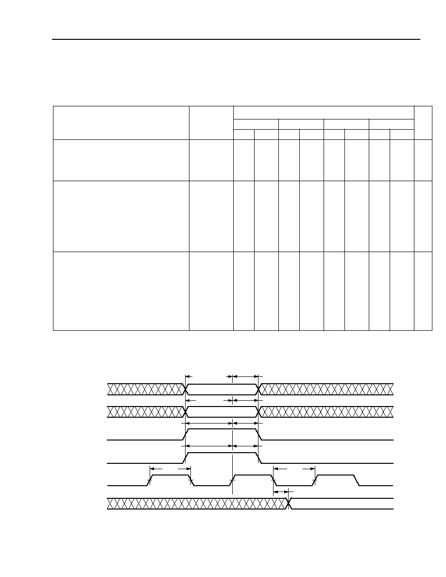
Table 44. Synchronous Memory Write Characteristics
OR3Cxx Commercial: VDD = 5.0 V ± 5%, 0 °C
< TA < 70 °C; Industrial: VDD = 5.0 V ± 10%, –40 °C < TA < +85 °C.
OR3Txxx Commercial: VDD = 3.0 V to 3.6 V, 0 °C
< TA < 70 °C; Industrial: VDD = 3.0 V to 3.6 V, –40 °C < TA < +85 °C.
* The RAM is written on the inactive clock edge following the active edge that latches the address, data, and control signals.
Note: The table shows worst-case delays. ispLEVER reports the delays for individual paths within a group of paths representing the same tim-
ing parameter and may accurately report delays that are less than those listed.
5-4621(F)
Figure 65. Synchronous Memory Write Characteristics
Parameter
Symbol
Speed
Unit
-4
-5
-6
-7
Min
Max
Min
Max
Min
Max
Min
Max
Write Operation for RAM Mode:
Maximum Frequency
Clock Low Time
Clock High Time
Clock to Data Valid (CLK to F[6, 4, 2, 0])*
SMCLK_FRQ
SMCLKL_MPW
SMCLKH_MPW
MEM_DEL
—
2.34
3.79
—
151.00
—
10.00
—
1.80
2.77
—
197.00
—
7.14
—
1.32
2.13
—
254.00
—
5.00
—
1.05
1.62
—
315.00
4.08
MHz
ns
Write Operation Setup Time:
Address to Clock (CIN to CLK)
Address to Clock (DIN[7, 5, 3, 1] to CLK)
Data to Clock (DIN[6, 4, 2, 0] to CLK)
Write Enable (WREN) to Clock (ASWE to CLK)
Write-port Enable 0 (WPE0) to Clock (CE to
CLK)
Write-port Enable 1 (WPE1) to Clock (LSR to
CLK)
WA4_SET
WA_SET
WD_SET
WE_SET
WPE0_SET
WPE1_SET
1.25
0.72
0.02
0.18
2.25
2.79
—
0.99
0.52
0.06
0.16
1.69
2.13
—
0.71
0.35
0.00
0.14
1.16
1.58
—
0.58
0.28
0.00
0.12
0.84
1.31
—
ns
Write Operation Hold Time:
Address from Clock (CIN from CLK)
Address from Clock (DIN[7, 5, 3, 1] from CLK)
Data from Clock (DIN[6, 4, 2, 0] from CLK)
Write Enable (WREN) from Clock (ASWE from
CLK)
Write-port Enable 0 (WPE0) from Clock (CE
from CLK)
Write-port Enable 1 (WPE1) from Clock (LSR
from CLK)
WA4_HLD
WA_HLD
WD_HLD
WE_HLD
WPE0_HLD
WPE1_HLD
0.00
0.59
0.03
0.00
—
0.00
0.42
0.00
—
0.00
0.40
0.08
0.00
—
0.00
0.32
0.06
0.00
—
ns
CK
F[6, 4, 2, 0]
CIN, DIN[7, 5, 3, 1]
DIN[6, 4, 2, 0]
MEM_DEL
WA4_SET
ASWE (WREN)
CE (WPE0),
TSCH
TSCL
WA4_HLD
WD_SET
WD_HLD
WE_SET
WE_HLD
WPE0_SET
WPE0_HLD
WA_SET
WA_HLD
WPE1_SET
WPE1_HLD
LSR (WPE1)
Select
devices
have
been
discontinued.
See
Ordering
Information
section
for
product
status.
相关PDF资料 |
PDF描述 |
|---|---|
| OR3T306S240I-DB | FPGA, 196 CLBS, 48000 GATES, PQFP240 |
| OR3T307S240-DB | FPGA, 196 CLBS, 48000 GATES, PQFP240 |
| OR3T556PS240-DB | FPGA, 324 CLBS, 80000 GATES, PQFP240 |
| OR3T806PS240-DB | FPGA, 484 CLBS, 116000 GATES, PQFP240 |
| OR3T807PS240-DB | FPGA, 484 CLBS, 116000 GATES, PQFP240 |
相关代理商/技术参数 |
参数描述 |
|---|---|
| OR3T125-7PS208I | 制造商:AGERE 制造商全称:AGERE 功能描述:3C and 3T Field-Programmable Gate Arrays |
| OR3T125-7PS240 | 制造商:AGERE 制造商全称:AGERE 功能描述:3C and 3T Field-Programmable Gate Arrays |
| OR3T1257PS240-DB | 功能描述:FPGA - 现场可编程门阵列 6272 LUT 342 I/O RoHS:否 制造商:Altera Corporation 系列:Cyclone V E 栅极数量: 逻辑块数量:943 内嵌式块RAM - EBR:1956 kbit 输入/输出端数量:128 最大工作频率:800 MHz 工作电源电压:1.1 V 最大工作温度:+ 70 C 安装风格:SMD/SMT 封装 / 箱体:FBGA-256 |
| OR3T125-7PS240I | 制造商:AGERE 制造商全称:AGERE 功能描述:3C and 3T Field-Programmable Gate Arrays |
| OR3T20 | 制造商:AGERE 制造商全称:AGERE 功能描述:3C and 3T Field-Programmable Gate Arrays |
发布紧急采购,3分钟左右您将得到回复。