参数资料
| 型号: | X40414V8-A |
| 厂商: | Intersil |
| 文件页数: | 10/24页 |
| 文件大小: | 0K |
| 描述: | IC VOLTAGE MON DUAL W/SUP 8TSSOP |
| 标准包装: | 100 |
| 类型: | 多压监控器 |
| 监视电压数目: | 2 |
| 输出: | 开路漏极,推挽式 |
| 复位: | 高有效/低有效 |
| 复位超时: | 可调节/可选择 |
| 电压 - 阀值: | 1.3V,2.9V |
| 工作温度: | 0°C ~ 70°C |
| 安装类型: | 表面贴装 |
| 封装/外壳: | 8-TSSOP(0.173",4.40mm 宽) |
| 供应商设备封装: | 8-TSSOP |
| 包装: | 管件 |
�� �
�
�X40410,� X40411,� X40414,� X40415�
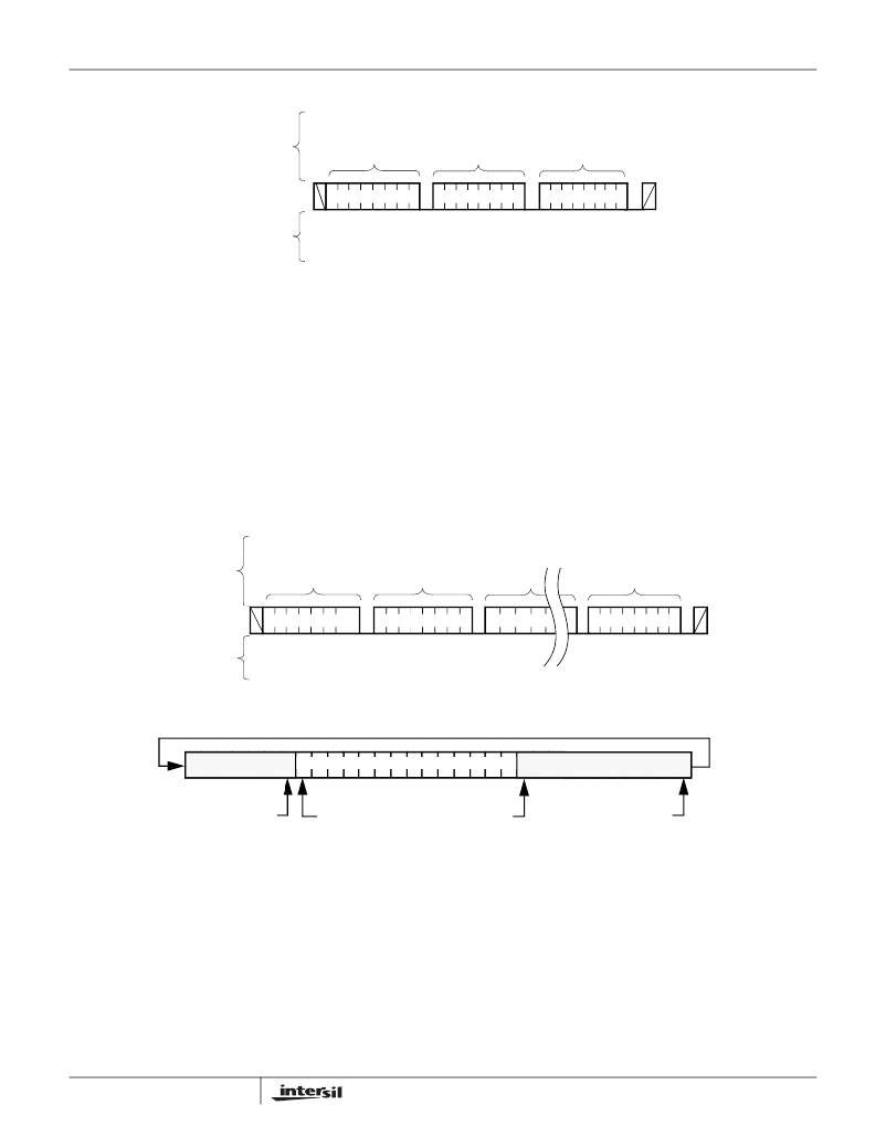
�Figure� 9.� Byte� Write� Sequence�
�Signals� from�
�the� Master�
�S�
�t�
�a�
�r�
�t�
�Slave�
�Address�
�Byte�
�Address�
�Data�
�S�
�t�
�o�
�p�
�SDA� Bus�
�0�
�Signals� from�
�the� Slave�
�A�
�C�
�K�
�A�
�C�
�K�
�A�
�C�
�K�
�Page� Write�
�The� device� is� capable� of� a� page� write� operation.� It� is�
�initiated� in� the� same� manner� as� the� byte� write� opera-�
�tion;� but� instead� of� terminating� the� write� cycle� after� the�
�first� data� byte� is� transferred,� the� master� can� transmit�
�an� unlimited� number� of� 8-bit� bytes.� After� the� receipt� of�
�each� byte,� the� device� will� respond� with� an� acknowl-�
�edge,� and� the� address� is� internally� incremented� by�
�one.� The� page� address� remains� constant.� When� the�
�counter� reaches� the� end� of� the� page,� it� “rolls� over”� and�
�goes� back� to� ‘0’� on� the� same� page.�
�Figure� 10.� Page� Write� Operation�
�This� means� that� the� master� can� write� 16� bytes� to� the�
�page� starting� at� any� location� on� that� page.� If� the� master�
�begins� writing� at� location� 10,� and� loads� 12� bytes,� then�
�the� first� 6� bytes� are� written� to� locations� 10� through� 15,�
�and� the� last� 6� bytes� are� written� to� locations� 0� through� 5.�
�Afterwards,� the� address� counter� would� point� to� location�
�6� of� the� page� that� was� just� written.� If� the� master� sup-�
�plies� more� than� 16� bytes� of� data,� then� new� data� over-�
�writes� the� previous� data,� one� byte� at� a� time.�
�Signals� from�
�the� Master�
�S�
�t�
�a�
�r�
�t�
�Slave�
�Address�
�Byte�
�Address�
�Data�
�(1)�
�(1� ≤� n� ≤� 16)�
�Data�
�(n)�
�S�
�t�
�o�
�p�
�SDA� Bus�
�1� 0� 1� 0� 0� 0�
�0�
�Signals� from�
�the� Slave�
�A�
�C�
�K�
�A�
�C�
�K�
�A�
�C�
�K�
�A�
�C�
�K�
�Figure� 11.� Writing� 12� bytes� to� a� 16-byte� page� starting� at� location� 10.�
�7� Bytes�
�5� Bytes�
�address�
�=6�
�address� pointer�
�ends� here�
�Addr� =� 7�
�address�
�10�
�address�
�n-1�
�The� master� terminates� the� Data� Byte� loading� by� issuing�
�a� stop� condition,� which� causes� the� device� to� begin� the�
�nonvolatile� write� cycle.� As� with� the� byte� write� operation,�
�10�
�all� inputs� are� disabled� until� completion� of� the� internal�
�write� cycle.� See� Figure� 10� for� the� address,� acknowl-�
�edge,� and� data� transfer� sequence.�
�FN8116.0�
�March� 28,� 2005�
�相关PDF资料 |
PDF描述 |
|---|---|
| ESA35DTKT-S288 | CONN EDGECARD 70POS .125 EXTEND |
| GSC26DRYH-S13 | CONN EDGECARD 52POS .100 EXTEND |
| X40414S8I-CT1 | IC VOLTAGE MON DUAL W/SUP 8-SOIC |
| GMC26DRYH-S13 | CONN EDGECARD 52POS .100 EXTEND |
| X40414S8I-C | IC VOLTAGE MON DUAL W/SUP 8-SOIC |
相关代理商/技术参数 |
参数描述 |
|---|---|
| P89LPC932A1 | 制造商:PHILIPS 制造商全称:NXP Semiconductors 功能描述:8-Bit Microcontroller with accelerated two-clock 80C51 core 8kB 3V byte-erasable flash with 512-byte data EEPROM |
| P89LPC932A1FA | 制造商:PHILIPS 制造商全称:NXP Semiconductors 功能描述:8-Bit Microcontroller with accelerated two-clock 80C51 core 8kB 3V byte-erasable flash with 512-byte data EEPROM |
| P89LPC932A1FA,112 | 功能描述:8位微控制器 -MCU 8K FL/768B RAM/512B EE/CCU RoHS:否 制造商:Silicon Labs 核心:8051 处理器系列:C8051F39x 数据总线宽度:8 bit 最大时钟频率:50 MHz 程序存储器大小:16 KB 数据 RAM 大小:1 KB 片上 ADC:Yes 工作电源电压:1.8 V to 3.6 V 工作温度范围:- 40 C to + 105 C 封装 / 箱体:QFN-20 安装风格:SMD/SMT |
| P89LPC932A1FA,129 | 功能描述:8位微控制器 -MCU 8K FL/768B RAM/512B EE/CCU RoHS:否 制造商:Silicon Labs 核心:8051 处理器系列:C8051F39x 数据总线宽度:8 bit 最大时钟频率:50 MHz 程序存储器大小:16 KB 数据 RAM 大小:1 KB 片上 ADC:Yes 工作电源电压:1.8 V to 3.6 V 工作温度范围:- 40 C to + 105 C 封装 / 箱体:QFN-20 安装风格:SMD/SMT |
| P89LPC932A1FDH | 制造商:PHILIPS 制造商全称:NXP Semiconductors 功能描述:8-bit microcontroller with accelerated two-clock 80C51 core 8 kB 3 V byte-erasable flash with 512-byte data EEPROM |
发布紧急采购,3分钟左右您将得到回复。