- 您现在的位置:买卖IC网 > PDF目录369948 > PC28F256J3C-115 (Intel Corp.) Intel StrataFlash Memory (J3) PDF资料下载
参数资料
| 型号: | PC28F256J3C-115 |
| 厂商: | Intel Corp. |
| 英文描述: | Intel StrataFlash Memory (J3) |
| 中文描述: | 英特尔StrataFlash存储器(J3) |
| 文件页数: | 36/72页 |
| 文件大小: | 905K |
| 代理商: | PC28F256J3C-115 |
第1页第2页第3页第4页第5页第6页第7页第8页第9页第10页第11页第12页第13页第14页第15页第16页第17页第18页第19页第20页第21页第22页第23页第24页第25页第26页第27页第28页第29页第30页第31页第32页第33页第34页第35页当前第36页第37页第38页第39页第40页第41页第42页第43页第44页第45页第46页第47页第48页第49页第50页第51页第52页第53页第54页第55页第56页第57页第58页第59页第60页第61页第62页第63页第64页第65页第66页第67页第68页第69页第70页第71页第72页
256-Mbit J3 (x8/x16)
36
Datasheet
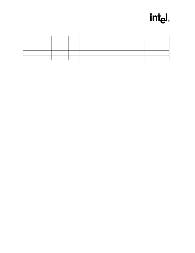
Clear Block Lock-Bits
SCS
2
Write
X
0x60
Write
X
0xD0
1,15
Protection Program
2
Write
X
0xC0
Write
PA
PD
1
NOTES:
1. Commands other than those shown above are reserved by Intel for future device implementations and should not be used.
2. The Basic Command Set (BCS) is the same as the 28F008SA Command Set or Intel Standard Command Set. The Scalable
Command Set (SCS) is also referred to as the Intel Extended Command Set.
3. Bus operations are defined in
Table 12
.
4. X = Any valid address within the device.
BA = Address within the block.
IA = Identifier Code Address: see
Table 17
.
QA = Query database Address.
PA = Address of memory location to be programmed.
RCD = Data to be written to the read configuration register. This data is presented to the device on A[16:1]; all other address
inputs
are ignored.
5. ID = Data read from Identifier Codes.
QD = Data read from Query database.
SRD = Data read from Status Register. See
Table 18
for a description of the Status Register bits.
PD = Data to be programmed at location PA. Data is latched on the rising edge of WE#.
CC = Configuration Code.
6. The upper byte of the data bus (D[15:8]) during command writes is a “Don’t Care” in x16 operation.
7. Following the Read Identifier Codes command, read operations access manufacturer, device and block lock codes. See
Section 10.2
for read identifier code data.
8. If the WSM is running, only D7 is valid; D[15:8] and D[6:0] float, which places them in a high-impedance state.
9. After the Write to Buffer command is issued check the XSR to make sure a buffer is available for writing.
10.The number of bytes/words to be written to the Write Buffer = N + 1, where N = byte/word count argument. Count ranges on
this device for byte mode are N = 00H to N = 1FH and for word mode are N = 0x00 to N = 0x0F. The third and consecutive
bus cycles, as determined by N, are for writing data into the Write Buffer. The Confirm command (0xD0) is expected after
exactly N + 1 write cycles; any other command at that point in the sequence aborts the write to buffer operation. See
Figure
18, “Write to Buffer Flowchart” on page 59
for additional information
11.The write to buffer or erase operation does not begin until a Confirm command (0xD0) is issued.
12.Attempts to issue a block erase or program to a locked block.
13.Either 0x40 or 0x10 are recognized by the WSM as the byte/word program setup.
14.Program suspends can be issued after either the Write-to-Buffer or Word/Byte-Program operation is initiated.
15.The clear block lock-bits operation simultaneously clears all block lock-bits.
Table 14. Command Bus-Cycle Definitions (Sheet 2 of 2)
Command
Scalable or
Basic
Command
Set
(2)
Bus
Cycles
Req’d.
First Bus Cycle
Second Bus Cycle
Notes
Oper
(3)
Addr
(4)
Data
(5,6)
Oper
(3)
Addr
(4)
Data
(5,6)
相关PDF资料 |
PDF描述 |
|---|---|
| PC28F128J3C-115 | Intel StrataFlash Memory (J3) |
| PC28F640J3C-115 | Intel StrataFlash Memory (J3) |
| PC28F320J3C-115 | Intel StrataFlash Memory (J3) |
| PC28F128J3C-120 | Intel StrataFlash Memory (J3) |
| PC28F128J3C-125 | Intel StrataFlash Memory (J3) |
相关代理商/技术参数 |
参数描述 |
|---|---|
| PC28F256J3C-120 | 制造商:INTEL 制造商全称:Intel Corporation 功能描述:Intel StrataFlash Memory (J3) |
| PC28F256J3C125 | 制造商:INTEL 制造商全称:Intel Corporation 功能描述:Intel StrataFlash?? Memory |
| PC28F256J3C-125 | 制造商:INTEL 制造商全称:Intel Corporation 功能描述:Intel StrataFlash Memory (J3) |
| PC28F256J3C125 S B93 | 制造商:Intel 功能描述: |
| PC28F256J3C-150 | 制造商:INTEL 制造商全称:Intel Corporation 功能描述:Intel StrataFlash Memory (J3) |
发布紧急采购,3分钟左右您将得到回复。