- 您现在的位置:买卖IC网 > PDF目录369948 > PC28F256J3C-115 (Intel Corp.) Intel StrataFlash Memory (J3) PDF资料下载
参数资料
| 型号: | PC28F256J3C-115 |
| 厂商: | Intel Corp. |
| 英文描述: | Intel StrataFlash Memory (J3) |
| 中文描述: | 英特尔StrataFlash存储器(J3) |
| 文件页数: | 40/72页 |
| 文件大小: | 905K |
| 代理商: | PC28F256J3C-115 |
第1页第2页第3页第4页第5页第6页第7页第8页第9页第10页第11页第12页第13页第14页第15页第16页第17页第18页第19页第20页第21页第22页第23页第24页第25页第26页第27页第28页第29页第30页第31页第32页第33页第34页第35页第36页第37页第38页第39页当前第40页第41页第42页第43页第44页第45页第46页第47页第48页第49页第50页第51页第52页第53页第54页第55页第56页第57页第58页第59页第60页第61页第62页第63页第64页第65页第66页第67页第68页第69页第70页第71页第72页
256-Mbit J3 (x8/x16)
40
Datasheet
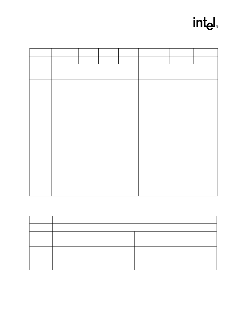
Table 18. Status Register Definitions
WSMS
ESS
ECLBS
PSLBS
VPENS
PSS
DPS
R
bit 7
bit 6
bit 5
bit 4
bit 3
bit2
bit 1
bit 0
High Z
When
Busy
Status Register Bits
Notes
No
Yes
Yes
Yes
Yes
Yes
Yes
Yes
SR.7 = WRITE STATE MACHINE STATUS
1 = Ready
0 = Busy
SR.6 = ERASE SUSPEND STATUS
1 = Block Erase Suspended
0 = Block Erase in Progress/Completed
SR.5 = ERASE AND CLEAR LOCK-BITSSTATUS
1 = Error in Block Erasure or Clear Lock-Bits
0 = Successful Block Erase or Clear Lock-Bits
SR.4 = PROGRAM AND SET LOCK-BIT STATUS
1 = Program Error / Error in Setting Lock-Bit
0 = Successful Program/Set Block Lock Bit
SR.3 = PROGRAMMING VOLTAGE STATUS
1 = Low Programming Voltage Detected, Operation
Aborted
0 = Programming Voltage OK
SR.2 = PROGRAM SUSPEND STATUS
1 = Program suspended
0 = Program in progress/completed
SR.1 = DEVICE PROTECT STATUS
1 = Block Lock-Bit Detected, Operation Abort
0 = Unlock
SR0 = RESERVED FOR FUTURE ENHANCEMENTS
Check STS or SR.7 to determine block erase,
program, or lock-bit configuration completion.
SR[6:0] are not driven while SR.7 = “0.”
If both SR.5 and SR.4 are “1”s after a block erase or
lock-bit configuration attempt, an improper
command sequence was entered.
SR.3 does not provide a continuous programming
voltage level indication. The WSM interrogates and
indicates the programming voltage level only after
Block Erase, Program, Set Block Lock-Bit, or Clear
Block Lock-Bits command sequences.
SR.1 does not provide a continuous indication of
block lock-bit values. The WSM interrogates the
block lock-bits only after Block Erase, Program, or
Lock-Bit configuration command sequences. It
informs the system, depending on the attempted
operation, if the block lock-bit is set. Read the block
lock configuration codes using the Read Identifier
Codes command to determine block lock-bit status.
SR0 is reserved for future use and should be
masked when polling the Status Register.
Table 19. Extended Status Register Definitions
WBS
Reserved
bit 7
Bits 6 -- 0
High Z
When
Busy
Status Register Bits
Notes
No
Yes
XSR.7 = WRITE BUFFER STATUS
1 = Write buffer available
0 = Write buffer not available
XSR.6–XSR0 = RESERVED FOR FUTURE
ENHANCEMENTS
After a Buffer-Write command, XSR.7 = 1 indicates
that a Write Buffer is available.
SR[6:0] are reserved for future use and should be
masked when polling the Status Register.
相关PDF资料 |
PDF描述 |
|---|---|
| PC28F128J3C-115 | Intel StrataFlash Memory (J3) |
| PC28F640J3C-115 | Intel StrataFlash Memory (J3) |
| PC28F320J3C-115 | Intel StrataFlash Memory (J3) |
| PC28F128J3C-120 | Intel StrataFlash Memory (J3) |
| PC28F128J3C-125 | Intel StrataFlash Memory (J3) |
相关代理商/技术参数 |
参数描述 |
|---|---|
| PC28F256J3C-120 | 制造商:INTEL 制造商全称:Intel Corporation 功能描述:Intel StrataFlash Memory (J3) |
| PC28F256J3C125 | 制造商:INTEL 制造商全称:Intel Corporation 功能描述:Intel StrataFlash?? Memory |
| PC28F256J3C-125 | 制造商:INTEL 制造商全称:Intel Corporation 功能描述:Intel StrataFlash Memory (J3) |
| PC28F256J3C125 S B93 | 制造商:Intel 功能描述: |
| PC28F256J3C-150 | 制造商:INTEL 制造商全称:Intel Corporation 功能描述:Intel StrataFlash Memory (J3) |
发布紧急采购,3分钟左右您将得到回复。