- 您现在的位置:买卖IC网 > PDF目录369948 > PC28F256J3C-115 (Intel Corp.) Intel StrataFlash Memory (J3) PDF资料下载
参数资料
| 型号: | PC28F256J3C-115 |
| 厂商: | Intel Corp. |
| 英文描述: | Intel StrataFlash Memory (J3) |
| 中文描述: | 英特尔StrataFlash存储器(J3) |
| 文件页数: | 50/72页 |
| 文件大小: | 905K |
| 代理商: | PC28F256J3C-115 |
第1页第2页第3页第4页第5页第6页第7页第8页第9页第10页第11页第12页第13页第14页第15页第16页第17页第18页第19页第20页第21页第22页第23页第24页第25页第26页第27页第28页第29页第30页第31页第32页第33页第34页第35页第36页第37页第38页第39页第40页第41页第42页第43页第44页第45页第46页第47页第48页第49页当前第50页第51页第52页第53页第54页第55页第56页第57页第58页第59页第60页第61页第62页第63页第64页第65页第66页第67页第68页第69页第70页第71页第72页
256-Mbit J3 (x8/x16)
50
Datasheet
14.0
Special Modes
This section describes how to read the status, ID, and CFI registers. This section also details how to
configure the STS signal.
14.1
Set Read Configuration Register Command
This command is no longer supported on J3A or J3C. The J3A device will ignore this command,
while the J3C device will
result in an invalid command sequence (SR.4 and SR.5 =1).
14.2
Status (STS)
The Status (STS) signal can be configured to different states using the Configuration command.
Once the STS signal has been configured, it remains in that configuration until another
configuration command is issued or RP# is asserted low. Initially, the STS signal defaults to RY/
BY# operation where RY/BY# low indicates that the WSM is busy. RY/BY# high indicates that the
state machine is ready for a new operation or suspended.
Table 22, “STS Configuration Coding
Definitions” on page 50
displays the possible STS configurations.
To reconfigure the Status (STS) signal to other modes, the Configuration command is given
followed by the desired configuration code. The three alternate configurations are all pulse mode
for use as a system interrupt as described below. For these configurations, bit 0 controls Erase
Complete interrupt pulse, and bit 1 controls Program Complete interrupt pulse. Supplying the 0x00
configuration code with the Configuration command resets the STS signal to the default RY/BY#
level mode. The possible configurations and their usage are described in
Table 22, “STS
Configuration Coding Definitions” on page 50
. The Configuration command may only be given
when the device is not busy or suspended. Check SR.7 for device status. An invalid configuration
code will result in both SR.4 and SR.5 being set. When configured in one of the pulse modes, the
STS signal pulses low with a typical pulse width of 250 ns.
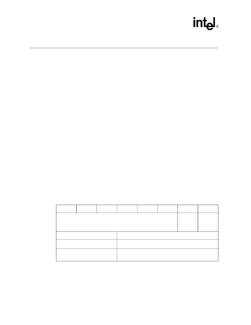
Table 22. STS Configuration Coding Definitions
D7
D6
D5
D4
D3
D2
D1
D0
Reserved
Pulse on
Program
Complete
(1)
Pulse on
Erase
Complete
(1)
D[1:0]
= STS Configuration Codes
Notes
00 = default, level mode;
device ready indication
Used to control HOLD to a memory controller to prevent accessing a
flash memory subsystem while any flash device's WSM is busy.
01 = pulse on Erase Complete
Used to generate a system interrupt pulse when any flash device in
an array has completed a block erase. Helpful for reformatting blocks
after file system free space reclamation or “cleanup.”
相关PDF资料 |
PDF描述 |
|---|---|
| PC28F128J3C-115 | Intel StrataFlash Memory (J3) |
| PC28F640J3C-115 | Intel StrataFlash Memory (J3) |
| PC28F320J3C-115 | Intel StrataFlash Memory (J3) |
| PC28F128J3C-120 | Intel StrataFlash Memory (J3) |
| PC28F128J3C-125 | Intel StrataFlash Memory (J3) |
相关代理商/技术参数 |
参数描述 |
|---|---|
| PC28F256J3C-120 | 制造商:INTEL 制造商全称:Intel Corporation 功能描述:Intel StrataFlash Memory (J3) |
| PC28F256J3C125 | 制造商:INTEL 制造商全称:Intel Corporation 功能描述:Intel StrataFlash?? Memory |
| PC28F256J3C-125 | 制造商:INTEL 制造商全称:Intel Corporation 功能描述:Intel StrataFlash Memory (J3) |
| PC28F256J3C125 S B93 | 制造商:Intel 功能描述: |
| PC28F256J3C-150 | 制造商:INTEL 制造商全称:Intel Corporation 功能描述:Intel StrataFlash Memory (J3) |
发布紧急采购,3分钟左右您将得到回复。