- 您现在的位置:买卖IC网 > PDF目录11447 > PIC18F86J16T-I/PT (Microchip Technology)IC PIC MCU FLASH 48KX16 80TQFP PDF资料下载
参数资料
| 型号: | PIC18F86J16T-I/PT |
| 厂商: | Microchip Technology |
| 文件页数: | 61/107页 |
| 文件大小: | 0K |
| 描述: | IC PIC MCU FLASH 48KX16 80TQFP |
| 产品培训模块: | Asynchronous Stimulus PIC18 J Series MCU Overview |
| 标准包装: | 1,200 |
| 系列: | PIC® 18F |
| 核心处理器: | PIC |
| 芯体尺寸: | 8-位 |
| 速度: | 48MHz |
| 连通性: | EBI/EMI,I²C,SPI,UART/USART |
| 外围设备: | 欠压检测/复位,LVD,POR,PWM,WDT |
| 输入/输出数: | 68 |
| 程序存储器容量: | 96KB(48K x 16) |
| 程序存储器类型: | 闪存 |
| RAM 容量: | 3930 x 8 |
| 电压 - 电源 (Vcc/Vdd): | 2 V ~ 3.6 V |
| 数据转换器: | A/D 15x10b |
| 振荡器型: | 内部 |
| 工作温度: | -40°C ~ 85°C |
| 封装/外壳: | 80-TQFP |
| 包装: | 带卷 (TR) |
| 配用: | AC162091-ND - HEADER MPLAB ICD2 18F87J11 64/80 MA180020-ND - MODULE PLUG-IN HPC EXPL 18F87J11 AC164328-ND - MODULE SKT FOR 80TQFP |
| 其它名称: | PIC18F86J16T-I/PTTR |
第1页第2页第3页第4页第5页第6页第7页第8页第9页第10页第11页第12页第13页第14页第15页第16页第17页第18页第19页第20页第21页第22页第23页第24页第25页第26页第27页第28页第29页第30页第31页第32页第33页第34页第35页第36页第37页第38页第39页第40页第41页第42页第43页第44页第45页第46页第47页第48页第49页第50页第51页第52页第53页第54页第55页第56页第57页第58页第59页第60页当前第61页第62页第63页第64页第65页第66页第67页第68页第69页第70页第71页第72页第73页第74页第75页第76页第77页第78页第79页第80页第81页第82页第83页第84页第85页第86页第87页第88页第89页第90页第91页第92页第93页第94页第95页第96页第97页第98页第99页第100页第101页第102页第103页第104页第105页第106页第107页
2007-2012 Microchip Technology Inc.
DS39778E-page 57
PIC18F87J11 FAMILY
5.2
Master Clear (MCLR)
The MCLR pin provides a method for triggering a hard
external Reset of the device. A Reset is generated by
holding the pin low. PIC18 extended microcontroller
devices have a noise filter in the MCLR Reset path
which detects and ignores small pulses.
The MCLR pin is not driven low by any internal Resets,
including the WDT.
5.3
Power-on Reset (POR)
A Power-on Reset condition is generated on-chip
whenever VDD rises above a certain threshold. This
allows the device to start in the initialized state when
VDD is adequate for operation.
To take advantage of the POR circuitry, tie the MCLR
pin through a resistor (1 k
to 10 k) to VDD. This will
eliminate external RC components usually needed to
create a Power-on Reset delay. A minimum rise rate for
time, see Figure 5-2.
When the device starts normal operation (i.e., exits the
Reset
condition),
device
operating
parameters
(voltage, frequency, temperature, etc.) must be met to
ensure operation. If these conditions are not met, the
device must be held in Reset until the operating
conditions are met.
Power-on Reset events are captured by the POR bit
(RCON<1>). The state of the bit is set to ‘0’ whenever
a Power-on Reset occurs; it does not change for any
other Reset event. POR is not reset to ‘1’ by any
hardware event. To capture multiple events, the user
manually resets the bit to ‘1’ in software following any
Power-on Reset.
5.4
Brown-out Reset (BOR)
The PIC18F87J11 family of devices incorporates a
simple Brown-out Reset function when the internal reg-
ulator is enabled (ENVREG pin is tied to VDD). Any
than time, TBOR, will reset the device. A Reset may or
may not occur if VDD falls below VBOR for less than
TBOR. The chip will remain in Brown-out Reset until
VDD rises above VBOR.
Once a Brown-out Reset has occurred, the Power-up
Timer will keep the chip in Reset for TPWRT
Power-up Timer is running, the chip will go back into a
Brown-out Reset and the Power-up Timer will be
initialized. Once VDD rises above VBOR, the Power-up
Timer will execute the additional time delay.
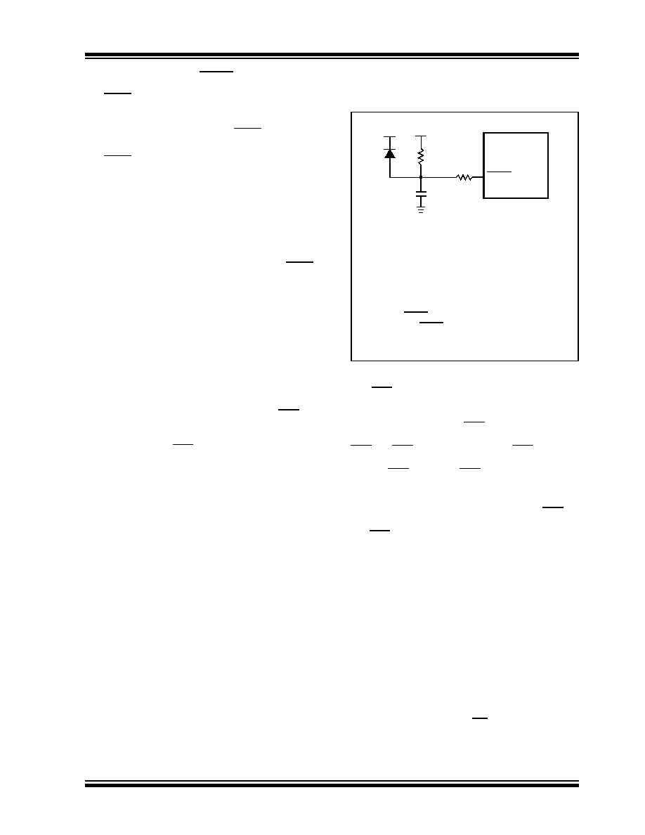
FIGURE 5-2:
EXTERNAL POWER-ON
RESET CIRCUIT (FOR
SLOW VDD POWER-UP)
5.4.1
DETECTING BOR
The BOR bit always resets to ‘0’ on any Brown-out
Reset or Power-on Reset event. This makes it difficult
to determine if a Brown-out Reset event has occurred
just by reading the state of BOR alone. A more reliable
method is to simultaneously check the state of both
POR and BOR. This assumes that the POR bit is reset
to ‘1’ in software immediately after any Power-on Reset
event. If BOR is ‘0’ while POR is ‘1’, it can be reliably
assumed that a Brown-out Reset event has occurred.
If the voltage regulator is disabled, Brown-out Reset
functionality is disabled. In this case, the BOR bit
cannot be used to determine a Brown-out Reset event.
The BOR bit is still cleared by a Power-on Reset event.
5.5
Configuration Mismatch (CM)
The Configuration Mismatch (CM) Reset is designed to
detect and attempt to recover from random, memory
corrupting events. These include Electrostatic Discharge
(ESD) events, which can cause widespread, single bit
changes throughout the device and result in catastrophic
failure.
In PIC18FXXJ Flash devices, the device Configuration
registers (located in the configuration memory space)
are continuously monitored during operation by
comparing their values to complimentary shadow reg-
isters. If a mismatch is detected between the two sets
of registers, a CM Reset automatically occurs. These
events are captured by the CM bit (RCON<5>). The
state of the bit is set to ‘0’ whenever a CM event occurs;
it does not change for any other Reset event.
Note 1:
External Power-on Reset circuit is required
only if the VDD power-up slope is too slow.
The diode, D, helps discharge the capacitor
quickly when VDD powers down.
2:
R < 40 k
is recommended to make sure that
the voltage drop across R does not violate
the device’s electrical specification.
3:
R1
1 k will limit any current flowing into
MCLR from external capacitor, C, in the event
of MCLR/VPP pin breakdown, due to
Electrostatic Discharge (ESD) or Electrical
Overstress (EOS).
C
R1
R
D
VDD
MCLR
PIC18F87J11
VDD
相关PDF资料 |
PDF描述 |
|---|---|
| PIC24FJ128GA006T-I/PT | IC PIC MCU FLASH 128K 64TQFP |
| PIC16LF872T-I/SS | IC MCU FLASH 2KX14 EE A/D 28SSOP |
| PIC16LF870T-I/SS | IC MCU FLASH 2KX14 EE A/D 28SSOP |
| VI-J4L-IY-B1 | CONVERTER MOD DC/DC 28V 50W |
| VI-J4K-IY-B1 | CONVERTER MOD DC/DC 40V 50W |
相关代理商/技术参数 |
参数描述 |
|---|---|
| PIC18F86J50-I/PT | 功能描述:8位微控制器 -MCU 64KB Flash 3936byte RAM RoHS:否 制造商:Silicon Labs 核心:8051 处理器系列:C8051F39x 数据总线宽度:8 bit 最大时钟频率:50 MHz 程序存储器大小:16 KB 数据 RAM 大小:1 KB 片上 ADC:Yes 工作电源电压:1.8 V to 3.6 V 工作温度范围:- 40 C to + 105 C 封装 / 箱体:QFN-20 安装风格:SMD/SMT |
| PIC18F86J50T-I/PT | 功能描述:8位微控制器 -MCU 64KB FLSH 3936Bs RAM USB 2.0 nanoWatt RoHS:否 制造商:Silicon Labs 核心:8051 处理器系列:C8051F39x 数据总线宽度:8 bit 最大时钟频率:50 MHz 程序存储器大小:16 KB 数据 RAM 大小:1 KB 片上 ADC:Yes 工作电源电压:1.8 V to 3.6 V 工作温度范围:- 40 C to + 105 C 封装 / 箱体:QFN-20 安装风格:SMD/SMT |
| PIC18F86J55-I/PT | 功能描述:8位微控制器 -MCU 96KB FLSH 3936Bs RAM USB 2.0 nanoWatt RoHS:否 制造商:Silicon Labs 核心:8051 处理器系列:C8051F39x 数据总线宽度:8 bit 最大时钟频率:50 MHz 程序存储器大小:16 KB 数据 RAM 大小:1 KB 片上 ADC:Yes 工作电源电压:1.8 V to 3.6 V 工作温度范围:- 40 C to + 105 C 封装 / 箱体:QFN-20 安装风格:SMD/SMT |
| PIC18F86J55T-I/PT | 功能描述:8位微控制器 -MCU 96KB FLSH 3936Bs RAM USB 2.0 nanoWatt RoHS:否 制造商:Silicon Labs 核心:8051 处理器系列:C8051F39x 数据总线宽度:8 bit 最大时钟频率:50 MHz 程序存储器大小:16 KB 数据 RAM 大小:1 KB 片上 ADC:Yes 工作电源电压:1.8 V to 3.6 V 工作温度范围:- 40 C to + 105 C 封装 / 箱体:QFN-20 安装风格:SMD/SMT |
| PIC18F86J60-I/PT | 功能描述:8位微控制器 -MCU 64KB FL 12KB RAM 10BASE-T RoHS:否 制造商:Silicon Labs 核心:8051 处理器系列:C8051F39x 数据总线宽度:8 bit 最大时钟频率:50 MHz 程序存储器大小:16 KB 数据 RAM 大小:1 KB 片上 ADC:Yes 工作电源电压:1.8 V to 3.6 V 工作温度范围:- 40 C to + 105 C 封装 / 箱体:QFN-20 安装风格:SMD/SMT |
发布紧急采购,3分钟左右您将得到回复。