参数资料
| 型号: | LTC3617EUDD#TRPBF |
| 厂商: | Linear Technology |
| 文件页数: | 13/20页 |
| 文件大小: | 0K |
| 描述: | IC REG SYNC 6A BUCK 24QFN |
| 标准包装: | 2,500 |
| 应用: | 转换器,DDR,DDR2,DDR3 |
| 输入电压: | 2.25 V ~ 5.5 V |
| 输出数: | 1 |
| 输出电压: | 可调至 0.5V |
| 工作温度: | -40°C ~ 125°C |
| 安装类型: | 表面贴装 |
| 封装/外壳: | 24-WFQFN 裸露焊盘 |
| 供应商设备封装: | 24-QFN(3x5) |
| 包装: | 带卷 (TR) |
�� �
�
�LTC3617�
�APPLICATIONS� INFORMATION�
�C� OUT� ≈�
�V� OUT� =�
�V� OUT� =�
�?� ?� 1� +�
�SincetheESRofaceramiccapacitorissolow,theinput�
�and� output� capacitor� must� instead� fulfill� a� charge� storage�
�requirement.� During� a� load� step,� the� output� capacitor� must�
�instantaneously� supply� the� current� until� the� feedback� loop�
�raises� the� switch� current� enough� to� support� the� load.� The�
�time� required� for� the� feedback� loop� to� respond� is� dependent�
�on� the� compensation� components� and� the� output� capaci-�
�tor� size.� Typically,� 3� to� 4� switching� cycles� are� required� to�
�respond� to� a� load� step,� but� only� in� the� first� cycle� does� the�
�output� drop� linearly.� The� output� droop,� V� DROOP� ,� is� usually�
�about� 2� to� 4� times� the� linear� drop� of� the� first� cycle;� however,�
�this� behavior� can� vary� depending� on� the� compensation�
�component� values.� Thus,� a� good� place� to� start� is� with� the�
�output� capacitor� size� of� approximately:�
�3.5� ?� ?� I� OUT�
�f� SW� ?� V� DROOP�
�This� is� only� an� approximation;� more� capacitance� may�
�be� needed� depending� on� the� duty� cycle� and� load� step�
�requirements.�
�In� most� applications,� the� input� capacitor� is� merely� required�
�to� supply� high� frequency� bypassing,� since� the� impedance�
�to� the� supply� is� very� low.�
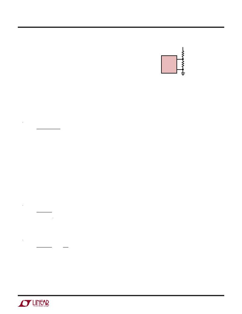
�Output� Voltage� Programming�
�In� most� applications,� V� OUT� is� connected� directly� to� V� FB� .�
�The� output� voltage� will� be� equal� to� one-half� of� the� voltage�
�on� the� VDDQIN� pin� for� this� case.�
�VDDQIN�
�2�
�If� a� different� output� relationship� is� desired,� an� external�
�resistor� divider� from� V� OUT� to� V� FB� can� be� used.� The� output�
�voltage� will� then� be� set� according� to� the� following� equation:�
�VDDQIN� ?� R2� ?�
�?�
�2� ?� R1� ?�
�V� OUT�
�R2�
�V� FB�
�LTC3617� R1�
�SGND�
�3617� F03�
�Figure� 3.� Setting� the� Output� Voltage�
�Internal� and� External� Compensation�
�The� regulator� loop� response� can� be� checked� by� looking� at�
�the� load� current� transient� response.� Switching� regulators�
�take� several� cycles� to� respond� to� a� step� in� DC� load� current.�
�When� a� load� step� occurs,� V� OUT� shifts� by� an� amount� equal�
�to� ?� I� LOAD� ?� ESR,� where� ESR� is� the� effective� series� resis� -�
�tance� of� C� OUT� .� ?� I� LOAD� also� begins� to� charge� or� discharge�
�C� OUT� ,� generating� the� feedback� error� signal� that� forces� the�
�regulator� to� adapt� to� the� current� change� and� return� V� OUT� to�
�its� steady-state� value.� During� this� recovery� time� V� OUT� can�
�be� monitored� for� excessive� overshoot� or� ringing,� which�
�would� indicate� a� stability� problem.� The� availability� of� the�
�ITH� pin� allows� the� transient� response� to� be� optimized� over�
�a� wide� range� of� output� capacitance.�
�The� ITH� external� components� (R� C� and� C� C� )� shown� in� Fig� -�
�ure� 1� provide� adequate� compensation� as� a� starting� point�
�for� most� applications.� The� values� can� be� modified� slightly�
�to� optimize� transient� response� once� the� final� PCB� layout�
�is� done� and� the� particular� output� capacitor� type� and� value�
�have� been� determined.� The� output� capacitors� need� to� be�
�selected� because� the� various� types� and� values� determine�
�the� loop� gain� and� phase.� The� gain� of� the� loop� will� be� in� -�
�creased� by� increasing� R� C� and� the� bandwidth� of� the� loop�
�will� be� increased� by� decreasing� C� C� .� If� R� C� is� increased� by�
�the� same� factor� that� C� C� is� decreased,� the� zero� frequency�
�will� be� kept� the� same,� thereby� keeping� the� phase� shift� the�
�same� in� the� most� critical� frequency� range� of� the� feedback�
�loop.� The� output� voltage� settling� behavior� is� related� to� the�
�stability� of� the� closed-loop� system.� The� external� capaci-�
�tor,� C� C1� ,� (Figure� 1)� is� not� needed� for� loop� stability,� but� it�
�helps� filter� out� any� high� frequency� noise� that� may� couple�
�onto� that� node.�
�3617fa�
�13�
�相关PDF资料 |
PDF描述 |
|---|---|
| HBC35DRES-S93 | CONN EDGECARD 70POS .100 EYELET |
| HMM08DRKF-S13 | CONN EDGECARD 16POS .156 EXTEND |
| HBM36DRKS | CONN EDGECARD 72POS DIP .156 SLD |
| GSC30DRYS-S93 | CONN EDGECARD 60POS DIP .100 SLD |
| GCM40DTBT | CONN EDGECARD 80POS R/A .156 SLD |
相关代理商/技术参数 |
参数描述 |
|---|---|
| PIC18LF4620T-I/ML | 功能描述:8位微控制器 -MCU 64KB 3968 RAM 36I/O RoHS:否 制造商:Silicon Labs 核心:8051 处理器系列:C8051F39x 数据总线宽度:8 bit 最大时钟频率:50 MHz 程序存储器大小:16 KB 数据 RAM 大小:1 KB 片上 ADC:Yes 工作电源电压:1.8 V to 3.6 V 工作温度范围:- 40 C to + 105 C 封装 / 箱体:QFN-20 安装风格:SMD/SMT |
| PIC18LF4620T-I/PT | 功能描述:8位微控制器 -MCU 64KB 3968 RAM 36I/O RoHS:否 制造商:Silicon Labs 核心:8051 处理器系列:C8051F39x 数据总线宽度:8 bit 最大时钟频率:50 MHz 程序存储器大小:16 KB 数据 RAM 大小:1 KB 片上 ADC:Yes 工作电源电压:1.8 V to 3.6 V 工作温度范围:- 40 C to + 105 C 封装 / 箱体:QFN-20 安装风格:SMD/SMT |
| PIC18LF4680-I/ML | 功能描述:8位微控制器 -MCU 64KB 3328 RAM w/ECAN RoHS:否 制造商:Silicon Labs 核心:8051 处理器系列:C8051F39x 数据总线宽度:8 bit 最大时钟频率:50 MHz 程序存储器大小:16 KB 数据 RAM 大小:1 KB 片上 ADC:Yes 工作电源电压:1.8 V to 3.6 V 工作温度范围:- 40 C to + 105 C 封装 / 箱体:QFN-20 安装风格:SMD/SMT |
| PIC18LF4680-I/P | 功能描述:8位微控制器 -MCU 64KB 3328 RAM w/ECAN RoHS:否 制造商:Silicon Labs 核心:8051 处理器系列:C8051F39x 数据总线宽度:8 bit 最大时钟频率:50 MHz 程序存储器大小:16 KB 数据 RAM 大小:1 KB 片上 ADC:Yes 工作电源电压:1.8 V to 3.6 V 工作温度范围:- 40 C to + 105 C 封装 / 箱体:QFN-20 安装风格:SMD/SMT |
| PIC18LF4680-I/P | 制造商:Microchip Technology Inc 功能描述:8-Bit Microcontroller IC |
发布紧急采购,3分钟左右您将得到回复。