参数资料
| 型号: | MIC29201-12WU |
| 厂商: | Micrel Inc |
| 文件页数: | 5/12页 |
| 文件大小: | 0K |
| 描述: | IC REG LDO 12V .4A TO-263-5 |
| 标准包装: | 50 |
| 稳压器拓扑结构: | 正,固定式 |
| 输出电压: | 12V |
| 输入电压: | 最高 26V |
| 电压 - 压降(标准): | 0.4V @ 400mA |
| 稳压器数量: | 1 |
| 电流 - 输出: | 400mA |
| 工作温度: | -40°C ~ 125°C |
| 安装类型: | 表面贴装 |
| 封装/外壳: | TO-263-6,D²Pak(5 引线+接片),TO-263BA |
| 供应商设备封装: | TO-263-5 |
| 包装: | 管件 |
| 产品目录页面: | 1107 (CN2011-ZH PDF) |
| 其它名称: | 576-2211 MIC29201-12WU-ND |
�� �
�
�MIC2920A/29201/29202/29204�
�Micrel,� Inc.�
�Notes:�
�General:�
�Note� 1:�
�Note� 2:�
�Note� 3:�
�Note� 4:�
�Note� 5:�
�Note� 6:�
�Note� 7:�
�Note� 8:�
�Note� 9:�
�Note� 10:�
�Note� 11:�
�Note� 12:�
�Devices� are� ESD� protected;� however,� handling� precautions� are� recommended.�
�Absolute� maximum� ratings� indicate� limits� beyond� which� damage� to� the� component� may� occur.� Electrical� speci?cations� do� not� apply� when�
�operating� the� device� outside� of� its� rated� operating� conditions.� The� maximum� allowable� power� dissipation� is� a� function� of� the� maximum�
�junction� temperature,� T� J� (MAX)� ,� the� junction-to-ambient� thermal� resistance,� θ� JA� ,� and� the� ambient� temperature,� T� A� .� The� maximum� allowable�
�power� dissipation� at� any� ambient� temperature� is� calculated� using:� P� (MAX)� =� (T� J(MAX)� –� T� A� )� /� θ� JA.� Exceeding� the� maximum� allowable� power�
�dissipation� will� result� in� excessive� die� temperature,� and� the� regulator� will� go� into� thermal� shutdown.� The� junction� to� ambient� thermal�
�resistance� of� the� MIC29204BM� is� 160°C/W� mounted� on� a� PC� board.�
�Output� voltage� temperature� coef?cient� is� de?ned� as� the� worst� case� voltage� change� divided� by� the� total� temperature� range.�
�Regulation� is� measured� at� constant� junction� temperature� using� low� duty� cycle� pulse� testing.� Changes� in� output� voltage� due� to� heating� effects�
�are� covered� by� the� thermal� regulation� speci?cation.�
�Dropout� Voltage� is� de?ned� as� the� input� to� output� differential� at� which� the� output� voltage� drops� 100mV� below� its� nominal� value� measured� at�
�1V� differential.� At� low� values� of� programmed� output� voltage,� the� minimum� input� supply� voltage� of� 4.3V� over� temperature� must� be� taken� into�
�account.� The� MIC2920A� operates� down� to� 2V� of� input� at� reduced� output� current� at� 25°C.�
�Ground� pin� current� is� the� regulator� quiescent� current.� The� total� current� drawn� from� the� supply� is� the� sum� of� the� load� current� plus� the� ground�
�pin� current.�
�The� MIC2920A� features� fold-back� current� limiting.� The� short� circuit� (V� OUT� =� 0V)� current� limit� is� less� than� the� maximum� current� with� normal�
�output� voltage.�
�Thermal� regulation� is� de?ned� as� the� change� in� output� voltage� at� a� time� T� after� a� change� in� power� dissipation� is� applied,� excluding� load� or�
�line� regulation� effects.� Speci?cations� are� for� a� 200mA� load� pulse� at� V� IN� =� 20V� (a� 4W� pulse)� for� T� =� 10ms.�
�V� REF� ≤� V� OUT� ≤� (V� IN� –� 1� V),� 4.3V� ≤� V� IN� ≤� 26V,� 1� mA� <� I� L� ≤400� mA,� T� J� ≤� T� J� MAX.�
�Comparator� thresholds� are� expressed� in� terms� of� a� voltage� differential� at� the� Adjust� terminal� below� the� nominal� reference� voltage� measured�
�at� 6V� input.� To� express� these� thresholds� in� terms� of� output� voltage� change,� multiply� by� the� error� ampli?er� gain� =� V� OUT� /V� REF� =� (R1� +� R2)/R2.�
�For� example,� at� a� programmed� output� voltage� of� 5V,� the� Error� output� is� guaranteed� to� go� low� when� the� output� drops� by� 95� mV� x� 5V/1.235� V�
�=� 384� mV.� Thresholds� remain� constant� as� a� percent� of� VOUT� as� VOUT� is� varied,� with� the� dropout� warning� occurring� at� typically� 5%� below�
�nominal,� 7.7%� guaranteed.�
�V� SHUTDOWN� ≥� 2V,� V� IN� ≤� 26V,V� OUT� =� 0,� with� Adjust� pin� tied� to� 5V� Tap� or� to� the� R1,� R2� junction� (see� Figure� 3)� with� R1� ≥� 150kΩ.�
�When� used� in� dual� supply� systems� where� the� regulator� load� is� returned� to� a� negative� supply,� the� output� voltage� must� be� diode� clamped� to�
�ground.�
�Maximum� positive� supply� voltage� of� 60V� must� be� of� limited� duration� (<� 100ms)� and� duty� cycle� (� ≤� 1%).� The� maximum� continuous� supply�
�voltage� is� 26V.�
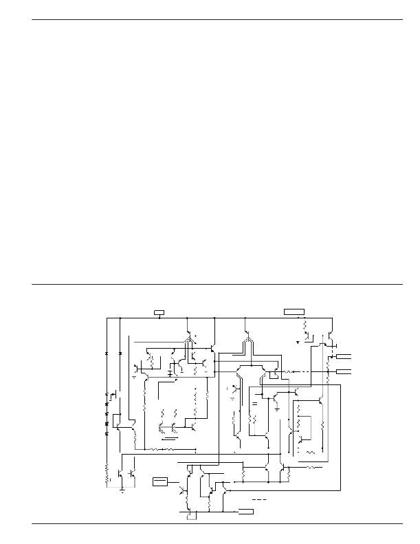
�Schematic� Diagram�
�IN�
�Q15A�
�Q15B�
�ADJUST�
�R18�
�20K� ?�
�Q26�
�Q24�
�Q9�
�Q25�
�OUT�
�Q6�
�10�
�Q3�
�Q1�
�R11�
�18�
�K� ?�
�C1�
�20�
�PF�
�Q4�
�Q5�
�Q2�
�R11�
�20.6�
�K� ?�
�Q7�
�Q8�
�Q16�
�Q17�
�Q14�
�R17�
�12� K� ?�
�R27�
�R28�
�SENSE�
�V� TAP�
�Q42�
�Q40�
�R1�
�20� K� ?�
�R2�
�50� K� ?�
�Q41�
�R5�
�180�
�K� ?�
�Q13�
�R6�
�140�
�K� ?�
�Q12�
�R8�
�31.4� K� ?�
�R9�
�27.8� K� ?�
�R10�
�150�
�K� ?�
�Q11�
�Q20�
�R12�
�110�
�K� ?�
�R13�
�100�
�K� ?�
�C2�
�40� PF�
�R14�
�350�
�K� ?�
�Q21�
�Q22�
�R15�
�100� K� ?�
�R16�
�30� K� ?�
�R17�
�10� ?�
�Q23�
�Q29�
�R30�
�30�
�K� ?�
�R3�
�50� K� ?�
�R4�
�13� K� ?�
�Q18�
�Q19�
�Q28�
�R21� 8� ?�
�50� K� ?�
�10� K� ?�
�ERROR�
�Q37�
�Q36�
�R22�
�150� K� ?�
�Q30� Q31�
�R24�
�50� K� ?�
�R23� 60� K� ?�
�SHDN�
�Q38�
�Q34�
�February� 2005�
�Q39�
�R26�
�60� K� ?�
�R25�
�2.8� K� ?�
�5�
�GND�
�D� E� NO� T� E� S� CO� NNE� CT� I� O� N� O� N�
�MIC2920A-XX� AND� MIC29201-XX�
�VERSIONS� ONLY�
�M9999-021505�
�相关PDF资料 |
PDF描述 |
|---|---|
| 200MXC820MEFCSN25X40 | CAP ALUM 820UF 200V 20% SNAP-IN |
| ASC17DREN-S93 | CONN EDGECARD 34POS .100 EYELET |
| ECC43DRTI-S734 | CONN EDGECARD 86POS DIP .100 SLD |
| ASC17DREH-S93 | CONN EDGECARD 34POS .100 EYELET |
| ESC20DRAI-S734 | CONN EDGECARD 40POS .100 R/A PCB |
相关代理商/技术参数 |
参数描述 |
|---|---|
| PIC24FJ256GB110T-I/PF | 功能描述:16位微控制器 - MCU 16B 16MIPS 256KB I/O RAM84 OTG RoHS:否 制造商:Texas Instruments 核心:RISC 处理器系列:MSP430FR572x 数据总线宽度:16 bit 最大时钟频率:24 MHz 程序存储器大小:8 KB 数据 RAM 大小:1 KB 片上 ADC:Yes 工作电源电压:2 V to 3.6 V 工作温度范围:- 40 C to + 85 C 封装 / 箱体:VQFN-40 安装风格:SMD/SMT |
| PIC24FJ256GB110T-I/PT | 功能描述:16位微控制器 - MCU 16B 16MIPS 256KB I/O RAM84 OTG RoHS:否 制造商:Texas Instruments 核心:RISC 处理器系列:MSP430FR572x 数据总线宽度:16 bit 最大时钟频率:24 MHz 程序存储器大小:8 KB 数据 RAM 大小:1 KB 片上 ADC:Yes 工作电源电压:2 V to 3.6 V 工作温度范围:- 40 C to + 85 C 封装 / 箱体:VQFN-40 安装风格:SMD/SMT |
| PIC24FJ256GB206-I | 制造商:MICROCHIP 制造商全称:Microchip Technology 功能描述:PIC24FJ256DA210 FAMILY, 64-100-Pin, 16-Bit Flash Microcontrollers with Graphics Controller and USB On-The-Go (OTG) |
| PIC24FJ256GB206-I/BG | 制造商:MICROCHIP 制造商全称:Microchip Technology 功能描述:64/100-Pin, 16-Bit Flash Microcontrollers with USB On-The-Go (OTG) |
| PIC24FJ256GB206-I/MR | 功能描述:16位微控制器 - MCU 16b 256KB Flash 96K RAM USB RoHS:否 制造商:Texas Instruments 核心:RISC 处理器系列:MSP430FR572x 数据总线宽度:16 bit 最大时钟频率:24 MHz 程序存储器大小:8 KB 数据 RAM 大小:1 KB 片上 ADC:Yes 工作电源电压:2 V to 3.6 V 工作温度范围:- 40 C to + 85 C 封装 / 箱体:VQFN-40 安装风格:SMD/SMT |
发布紧急采购,3分钟左右您将得到回复。