

产品信息
MP1593DN,MP1593,MPS中国代理商,mps代理商
深圳市万瑞尔科技有限公司
电话0755-2826-9789 83972660
电话0755-2826-9789 83972660
传真:0755-61390096
QQ4223-88688 EMAIL:CN58@WONREAL.NET
HTTP://WWW.WONREAL.NET
HTTP://WWW.WONREAL.NET
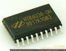
器件名称:MP1593
功能描述:4.75V to 28V Input, Up to 3A Output Step-Down DC/DC Converter
型号:MP1593DN MP3202DJ MP3302DJ 品牌:MPS
DC-DC (Step-Up)流—直流(升压)
Synchronous Switcher同步开关
MP3115、MP3120、MP3410
Non-Synchronous Switcher
MP1517、MP1522、MP1530、MP1531、MP1541、MP1542、MP3201、MP3208、MP3209
MP3212、MP3213、MP3216、MP3217、MP3900、MP9361
LDO Linear Regulators低压降线性调节器
MP2000、MP2002、MP2004、MP20041、MP20042、MP20045、MP2005、MP2007、MP2009
MP2016、MP2030、MP8801、MP8802、MP8903、MP8904
4.75V to 28V Input, Up to 3A Output Step-Down DC/DC Converter
TM MP1593 3A, 28V, 385KHz Step-Down Converter The Future of Analog IC Technology TM DESCRIPTION The MP1593 is a step-down regulator with an internal Power MOSFET. It achieves 3A continuous output current over a wide input supply range with excellent load and line regulation. Current mode operation provides fast transient response and eases loop stabilization. Fault condition protection includes cycle-by-cycle current limiting and thermal shutdown. Adjustable soft-start reduces the stress on the input source at turn-on. In shutdown mode the regulator draws 20?A of supply current. The MP1593 requires a minimum number of readily available external components to complete a 3A step down DC to DC converter solution. FEATURES ? ? ? ? ? ? ? ? ? ? ? ? ? ? ? ? ? ? ? ? 3A Output Current Programmable Soft-Start 100m? Internal Power MOSFET Switch Stable with Low ESR Output Ceramic Capacitors Up to 95% Efficiency 20?A Shutdown Mode Fixed 385KHz Frequency Thermal Shutdown Cycle-by-Cycle Over Current Protection Wide 4.75V to 28V Operating Input Range Output Adjustable from 1.22V Under Voltage Lockout Available in 8-Pin SOIC Package Distributed Power Systems Battery Chargers Pre-Regulator for Linear Regulators Flat Panel TVs Set-Top Boxes Cigarette Lighter Powered Devices DVD/PVR Devices APPLICATIONS EVALUATION BOARD REFERENCE Board Number EV1593DN-00A Dimensions 2.1”X x 1.3”Y x 0.4”Z “MPS” and “The Future of Analog IC Technology” are Trademarks of Monolithic Power Systems, Inc. TYPICAL APPLICATION INPUT 4.75V to 28V 2 IN 7 EN 8 1 BS 3 SW C5 10nF 100 95 Efficiency vs Load Current VIN = 9V VIN = 24V VIN = 12V EFFICIENCY (%) OFF ON MP1593 SS GND 4 FB COMP 6 OUTPUT 3.3V 3A 90 85 80 75 70 65 60 55 50 0 500 1000 1500 2000 2500 3000 3500 5 C6 (optional) C3 8.2nF D1 B340A MP1593_TAC01 LOAD CURRENT (mA) MP1593_TAC _EC01 MP1593 Rev. 1.8 1/6/2006 www.MonolithicPower.com MPS Proprietary Information. Unauthorized Photocopy and Duplication Prohibited. ? 2006 MPS. All Rights Reserved. 1 MP1593 – 3A, 28V, 385KHz STEP-DOWN CONVERTER PACKAGE REFERENCE TOP VIEW BS IN SW GND 1 2 3 4 8 7 6 5 SS EN COMP FB ABSOLUTE MAXIMUM RATINGS (1) Supply Voltage VIN ......................... –0.3V to 30V Switch Voltage VSW .............. –0.5V to VIN + 0.3V Boost Voltage VBS ..........VSW – 0.3V to VSW + 6V All Other Pins................................. –0.3V to +6V Junction Temperature...............................150°C Lead Temperature ....................................260°C Storage Temperature ...............–65°C to 150°C Recommended Operating Conditions (2) EXPOSED PAD ON BACKSIDE CONNECT TO PIN 4 MP1593_PD01_SOIC8N Input Voltage VIN ............................ 4.75V to 28V Ambient Operating Temp............. –40°C to +85°C Thermal Resistance Part Number* MP1593DN * Package SOIC8N (Exposed Pad) Temperature –40°C to +85°C (3) SOIC8N (w/Exposed Pad)...... 50 ...... 10... °C/W Notes: 1) Exceeding these ratings may damage the device. 2) The device is not guaranteed to function outside of its operating conditions. 3) Measured on approximately 1” square of 1 oz copper. θJA θJC For Tape & Reel, add suffix –Z (eg. MP1593DN–Z) For Lead Free, add suffix –LF (eg. MP1593DN–LF–Z) ELECTRICAL CHARACTERISTICS VIN = 12V, TA = +25°C, unless otherwise noted. Parameter Shutdown Supply Current Supply Current Feedback Voltage Error Amplifier Voltage Gain Error Amplifier Transconductance High Side Switch On Resistance Low Side Switch On Resistance High Side Switch Leakage Current Current Limit Current Sense to COMP Transconductance Oscillation Frequency Short Circuit Oscillation Frequency Maximum Duty Cycle Minimum Duty Cycle Symbol Condition VEN = 0V VEN = 2.6V, VFB = 1.4V VFB AEA GEA RDS(ON)1 RDS(ON)2 VEN = 0V, VSW = 0V 3.3 GCS fOSC1 fOSC2 DMAX DMIN VFB = 0V VFB = 1.0V VFB = 1.5V 335 25 ?ICOMP = ±10?A 500 4.75V ≤ VIN ≤ 28V VCOMP < 2V Min Typ 20 1.0 1.222 400 800 100 10 0 4.7 6.2 385 45 90 0 435 60 10 6.5 1120 140 Max 30 1.2 1.250 Units ?A mA V V/V ?A/V m? ? ?A A A/V KHz KHz % % 1.194 MP1593 Rev. 1.8 1/6/2006 www.MonolithicPower.com MPS Proprietary Information. Unauthorized Photocopy and Duplication Prohibited. ? 2006 MPS. All Rights Reserved. 2 MP1593 – 3A, 28V, 385KHz STEP-DOWN CONVERTER ELECTRICAL CHARACTERISTICS (continued) VIN = 12V, TA = +25°C, unless otherwise noted. Parameter EN Threshold Voltage Enable Pull Up Current Under Voltage Lockout Threshold Under Voltage Lockout Threshold Hysteresis Soft Start Period Thermal Shutdown Symbol Condition VEN = 0V VIN Rising Min 0.9 1.0 2.3 Typ 1.2 1.7 2.6 210 CSS = 0.1?F 10 160 Max 1.5 2.5 2.9 Units V ?A V mV ms °C TYPICAL PERFORMANCE CHARACTERISTICS Refer to Typical Application Schematic on Page 1 Feedback Voltage vs Temperature 1.245 1.235 1.225 1.215 1.205 1.195 -60 -40 -20 0 20 40 60 80 100 120 140 5.0 Peak Current Limit vs Temperature PEAK CURRENT LIMIT (A) 4.9 4.8 4.7 4.6 4.5 4.4 4.3 4.2 4.1 4.0 -50 -25 -0 25 50 75 100 125 150 MP1593-TPC02 Oscillation Frequency vs Temperature OSCILLATION FREQUENCY (KHz) 420 410 400 390 380 370 360 350 340 -60 -40 -20 0 20 40 60 80 100 120 140 FEEDBACK VOLTAGE (V) TEMPERATURE (°C) MP1593-TPC01 TEMPERATURE (°C) TEMPERATURE (°C) MP1593-TPC03 Soft-Start Waveforms Turn Off Waveforms VOUT 1V/Div. Load Transient Waveforms VOUT 100mV/Div. VOUT 1V/Div. IL 1A/Div. IL 1A/Div. IL 1A/Div. 4ms/Div. VIN = 12V, VOUT = 3.3V, 1A - 2A STEP MP1593-TPC04 MP1593-TPC05 MP1593-TPC-06 MP1593 Rev. 1.8 1/6/2006 www.MonolithicPower.com MPS Proprietary Information. Unauthorized Photocopy and Duplication Prohibited. ? 2006 MPS. All Rights Reserved. 3 MP1593 – 3A, 28V, 385KHz STEP-DOWN CONVERTER TYPICAL PERFORMANCE CHARACTERISTICS (continued) Refer to Typical Application Schematic on Page 1 Switching Waveforms IL 1A/Div. 100 95 90 Efficiency vs Load Current 100 Efficiency vs Load Current 95 90 VIN = 5V VIN = 9V VIN = 24V VIN = 12V EFFICIENCY (%) EFFICIENCY (%) VOUT 10mV/Div. VIN 100mV/Div. VSW 10V/Div. 85 80 75 70 65 60 55 50 0 500 1000 1500 2000 2500 3000 3500 85 80 75 70 65 60 55 50 0 VIN = 24V VIN = 12V 500 1000 1500 2000 2500 3000 3500 LOAD CURRENT (mA) MP1593-TPC07 MP1593_TPC08 LOAD CURRENT (mA) MP1593_TPC09 PIN FUNCTIONS Pin # Name Description 1 2 High-Side Gate Drive Boost Input. BS supplies the drive for the high-side N-Channel MOSFET switch. Connect a 10nF or greater capacitor from SW to BS to power the high side switch. Power Input. IN supplies the power to the IC, as well as the step-down converter switches. Drive IN IN with a 4.75V to 28V power source. Bypass IN to GND with a suitably large capacitor to eliminate noise on the input to the IC. See Input Capacitor section. Power Switching Output. SW is the switching node that supplies power to the output. Connect SW the output LC filter from SW to the output load. Note that a capacitor is required from SW to BS to power the high-side switch. GND Ground. (Note: Connect the exposed pad on backside to Pin 4). Feedback Input. FB senses the output voltage to regulate that voltage. Drive FB with a resistive FB voltage divider from the output voltage. The feedback threshold is 1.222V. See Setting the Output Voltage section. Compensation Node. COMP is used to compensate the regulation control loop. Connect a series COMP RC network from COMP to GND to compensate the regulation control loop. In some cases, an additional capacitor from COMP to GND is required. See Compensation section. Enable Input. EN is a digital input that turns the regulator on or off. Drive EN high to turn on the regulator, drive EN low to turn it off. An Under Voltage Lockout (UVLO) function can be EN implemented by the addition of a resistor divider from VIN to GND. For complete low current shutdown its needs to be less than 0.7V. For automatic startup, leave EN unconnected. Soft-Start Control Input. SS controls the soft-start period. Connect a capacitor from SS to GND SS to set the soft-start period. A 0.1?F capacitor sets the soft-start period to 10ms. To disable the soft-start feature, leave SS unconnected. BS 3 4 5 6 7 8 MP1593 Rev. 1.8 1/6/2006
查看更多
公司介绍
万瑞尔(荷兰)国际有限公司成立于1986年,几十年来万瑞尔在电子元件、无线电子、奢侈品与跨国投资等方面颇有建树。
电子元件方面:
现货库存: 万瑞尔(荷兰)国际有限公司是荷兰最大的电子元器件现货库存商之一,在总部阿姆斯特丹拥有四十三万余平方米的电子元器件现货存储仓库,拥有现货库存型号达到 五万三千余种,库存的产品类型有:运算放大器、逻辑电路、接口电路、电源电路、编解码器、通讯电路、传感器、显示电路、微处理器、存储器、单片机、可编程逻辑、功率驱动器等;库存的品牌有:NXP(PHILIP)、ATMEL、MICROCHIP、IDT、MAX、INTERSIL、AD、TI、BB、INTEL、AGILENT、ALLEGRO、NS、AMD、LATTICE、XILINX、MOT、ST、CYPRESS、ALTERA、ZILOG、INTERPOINT等。 总部所在为世界最大的海陆空中转港之一,物流业发达,能及时调动欧洲及美洲区域内2000家电子元器件现货库存商的现货库存,并与国际排名在前20名的电子元器件现货分销商保持着密切的合作关系 。
无线电子方面:
万瑞尔在世界各地拥有或控股五十余家无线电子科研及生产机构和二百多个销售办事处,产品涉及诸多无线安防设备,并在此领域拥有世界一流的技术和数以万计的发明专利。
金融方面 :
万瑞尔(荷兰)国际有限公司拥有考斯特钻石公司(Coster Diamonds B.V.) 9.5% 的股权 .
跨国投资方面 :
万瑞尔(荷兰)国际有限公司在南非拥有大型的钻石加工厂,业务遍部世界各地.
万瑞尔(荷兰)国际有限公司在亚洲拥有独立的销售中心,以中国香港为中心,业务覆盖整个大中华区域,以及整个亚洲地区.
查看更多


-
电话:0755-28269789|多线永不占线|买卖IC创始会员
联系人:刘先生/何小姐(2014十佳供应商) (先生)
QQ:
邮箱:cn58@wonreal.net
地址:深圳市福田区深南中路南光捷佳大厦18F
100%产品查看率
 会员等级
会员等级
 会员年限
会员年限