- 您现在的位置:买卖IC网 > PDF目录224961 > QT114-S IC-SMD-QPROX SENSOR PDF资料下载
参数资料
| 型号: | QT114-S |
| 英文描述: | IC-SMD-QPROX SENSOR |
| 中文描述: | 集成电路表面贴装,量研传感器 |
| 文件页数: | 5/12页 |
| 文件大小: | 310K |
| 代理商: | QT114-S |
The QT114 is a digital burst mode charge-transfer (QT)
sensor designed specifically for point level sensing; it
includes all hardware and signal processing functions
necessary to provide stable level sensing under a wide
variety of changing conditions. Only a single external
capacitor is required for operation.
Figure 1-1 shows a basic QT114 circuit using the device,
with conventional OUT drives and power supply connections.
The sensing electrode can be connected to a single-tier or
2-tier electrode as required.
Calibration is done by design, through adjustment of the
electrode sizes and the Cs capacitor. Only under rare
situations do QT114 circuits require calibration on an
individual basis, and the circuit can make provision for that.
1 - SIGNAL ACQUISITION
The QT114 employs a short, low duty cycle burst of
charge-transfer cycles to acquire its signal. Burst mode
permits power consumption in the low microamp range,
dramatically reduces RF emissions, lowers susceptibility to
EMI, and yet permits excellent response time. Internally the
signals are digitally processed to generate the required
output signals.
The QT switches and charge measurement hardware
functions are all internal to the QT114 (Figure 1-2). A 14-bit
single-slope switched capacitor ADC includes both the
required QT charge and transfer switches in a configuration
that provides direct ADC conversion. The burst length is
inversely proportional to the rate of charge buildup on Cs,
which in turn depends on the values of Cs, Cx, and Vcc. Vcc
is used as the charge reference voltage. Larger values of Cx
cause the charge transferred into Cs to accumulate more
rapidly. The trip points of the sensor can be changed by
altering Cs and Cx, the load capacitance. As a result, the
values of Cs, Cx, and Vcc should be fairly stable over the
expected operating temperature range.
Two fixed thresholds are used, one for low fluid level and the
other for high level; adjusting Cs and Cx to allow these to trip
at appropriate points is required by design, and if required
may be trimmed by an adjustment. Figure 1-1 shows the
optional potentiometer which can be used to fine-tune the
placement of these threshold points relative to the signal.
It is not necessary to use both detection threshold points; if
only single point sensing is desired, only the lower threshold
and OUT1 can be used, while ignoring OUT2.
Two option pins allow the selection of output polarity and the
insertion of a 'slosh filter' before the OUT pins, as shown in
Figure 1-1.
1.1 ELECTRODE DRIVE
The internal ADC treats Cs as a floating transfer capacitor;
as a direct result, the sense electrode can be connected to
either SNS1 or SNS2 with no performance difference. The
polarity of the charge buildup across Cs during a burst is the
same in either case. Cs must be of within a certain range for
proper operation.
It is possible to connect separate Cx and Cx’ loads to SNS1
and SNS2 simultaneously, although the result is no different
than if the loads were connected together at SNS2 (or
SNS1). It is important to limit the amount of stray
capacitance on both terminals, especially if the load Cx is
already large, for example by minimizing trace lengths and
widths so as not to exceed the Cx load specification and to
allow for a larger sensing electrode size if so desired.
The PCB traces, wiring, and any components associated
with or in contact with SNS1 and SNS2 will become
proximity sensitive and should be treated with caution.
1.2 THRESHOLD POINTS
The QT114 employs twin threshold points set at both
250 (for T1) and 150 counts (for T2) of acquisition
signal. The signal travels in an inverse direction:
increasing amounts of Cx reduce the signal level; the
baseline ('dry') signal should lie at 300 counts or
more under most conditions. Calibration details are
discussed fully in Section 3.2.
2 ELECTRODE DESIGN
The QT114 is designed to operate with a 'plateau'
sensor, having a substantial surface area at each
desired trip point, to create a capacitive 'step'.
As Figure 2-1 shows, a vertical strip sensor on the
outside of a container (or a vertical, insulated rod in
the fluid) will generate a long sloping signal. The
desired trip point 'T' is subject to a great deal of
variation in location if the sensing signal drifts much,
- 2 -
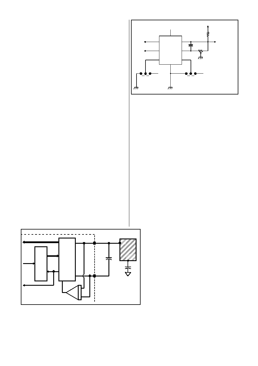
Figure 1-1 Standard mode options
OUT 2
Vdd
Cs
To 10x Scope Probe
To Electrode(s)
1M multi-turn
pot (optional)
2M (optional)
Gnd
OUT1
OUT2
FILT
Vcc
SNS2
SNS1
POL
POL: 1 = Active High
FILT: 1 = Slosh Filter
POLARITY
FILTER
1
2
3
45
6
7
8
OUT 1
Figure 1-2 Internal Switching & Timing
Cs
Cx
SNS2
SNS1
ELEC T RO DE
Si
n
g
le
-S
lo
p
e
1
4
-b
it
S
w
it
ched
C
a
p
a
ci
to
r
A
D
C
C harge
Am p
B
u
rs
tC
o
n
tro
lle
r
Result
Done
Start
相关PDF资料 |
PDF描述 |
|---|---|
| QT12C-SERIES | Peripheral IC |
| QT12E-SERIES | Peripheral IC |
| QT12HC-SERIES | Peripheral IC |
| QT12T-SERIES | Peripheral IC |
| QT14C-SERIES | Peripheral IC |
相关代理商/技术参数 |
参数描述 |
|---|---|
| QT115 | 制造商:QUANTUM 制造商全称:QUANTUM 功能描述:QT 11x Series Variations |
| QT115A-ISG | 功能描述:接口 - 专用 Integrated Circuit RoHS:否 制造商:Texas Instruments 产品类型:1080p60 Image Sensor Receiver 工作电源电压:1.8 V 电源电流:89 mA 最大功率耗散: 最大工作温度:+ 85 C 安装风格:SMD/SMT 封装 / 箱体:BGA-59 |
| QT115-D | 功能描述:SENSOR IC TOUCH/PROXMTY 1CH 8DIP RoHS:否 类别:集成电路 (IC) >> 数据采集 - 触摸屏控制器 系列:QProx™ 标准包装:96 系列:- 类型:- 触摸面板接口:- 输入数/键:- 分辨率(位):- 评估套件:* 数据接口:- 数据速率/采样率 (SPS,BPS):- 电压基准:- 电源电压:- 电流 - 电源:- 工作温度:- 安装类型:表面贴装 封装/外壳:16-TSSOP(0.173",4.40mm 宽) 供应商设备封装:16-TSSOP 包装:带卷 (TR) |
| QT115-DG | 制造商:Quantum Corp 功能描述:IC QPROX SENSOR DIP8 115 |
| QT115G1A-ISG | 功能描述:板机接口移动感应器和位置传感器 INTEGRATED-CIRCUIT RoHS:否 制造商:Panasonic Electric Works 封装 / 箱体:TO-5 感应距离:3 m 输出类型:Digital 电源电压-最大:6 V 电源电压-最小:2.3 V 电源电流: 最大工作温度:+ 60 C 封装:Bulk |
发布紧急采购,3分钟左右您将得到回复。