- 您现在的位置:买卖IC网 > PDF目录69322 > RK80530KZ017512 (INTEL CORP) 32-BIT, 1400 MHz, MICROPROCESSOR, CPGA370 PDF资料下载
参数资料
| 型号: | RK80530KZ017512 |
| 厂商: | INTEL CORP |
| 元件分类: | 微控制器/微处理器 |
| 英文描述: | 32-BIT, 1400 MHz, MICROPROCESSOR, CPGA370 |
| 封装: | FLIP CHIP, PGA-370 |
| 文件页数: | 13/94页 |
| 文件大小: | 1775K |
| 代理商: | RK80530KZ017512 |
第1页第2页第3页第4页第5页第6页第7页第8页第9页第10页第11页第12页当前第13页第14页第15页第16页第17页第18页第19页第20页第21页第22页第23页第24页第25页第26页第27页第28页第29页第30页第31页第32页第33页第34页第35页第36页第37页第38页第39页第40页第41页第42页第43页第44页第45页第46页第47页第48页第49页第50页第51页第52页第53页第54页第55页第56页第57页第58页第59页第60页第61页第62页第63页第64页第65页第66页第67页第68页第69页第70页第71页第72页第73页第74页第75页第76页第77页第78页第79页第80页第81页第82页第83页第84页第85页第86页第87页第88页第89页第90页第91页第92页第93页第94页
12
Datasheet
Intel Pentium III Processor with 512KB L2 Cache at 1.13GHz to 1.40GHz
2.6
Voltage Identification
There are five voltage identification (VID) pins on the PGA370 socket. These pins can be used to
support automatic selection of VCCCORE voltages. The VID pins for the Intel Pentium III
processor with 512KB L2 Cache are open drain signals versus opens or shorts found on the
previous Intel
specifications for the VID signals. This pull-up resistor may be either external logic on the
motherboard or internal to the Voltage Regulator.
The VID signals rely on a 3.3V pull-up resistor to set the signal to a logic high level. The VID pins
are needed to fully support voltage specification variations on current and future processors. The
voltage selection range for the processor is defined in Table 3. The VID25mV signal is a new
signal that allows the voltage regulator or voltage regulator module (VRM) to output voltage levels
in 25mV increment necessary for the Intel Pentium III processor with 512KB L2 Cache only.
The legacy Pentium III processor in the FC-PGA package will not have this VID25mV signal.
The VID25mV pin location is actually a Vss pin on the Pentium III processor (CPUID = 068xh).
By connecting the VID25mV signal to the Vss pin, it will disable the 25mV stepping granularity
output and the regulator will resort to 50mV stepping increment. The voltage regulator or VRM
must supply the voltage that is requested or disable itself.
In addition to the new signal “VID25mV”, the Intel Pentium III processor with 512KB L2
Cache will introduce a second new signal labeled as “VTT_PWRGD”. The VTT_PWRGD signal
informs the platform that the VID and BSEL signals are stable and should be sampled. During
power-up, the VID signals will be in an indeterminate state for a small period of time. The voltage
regulator or the VRM should not latch the VID signals until the VTT_PWRGD signal is asserted
by the VRM and sampled active. The assertion of the VTT_PWRGD signal indicates the VID
signals are stable and are driven to the final state by the processor. Refer to Figure 14 for power-up
timing sequence for the VTT_PWRGD and the VID signals.
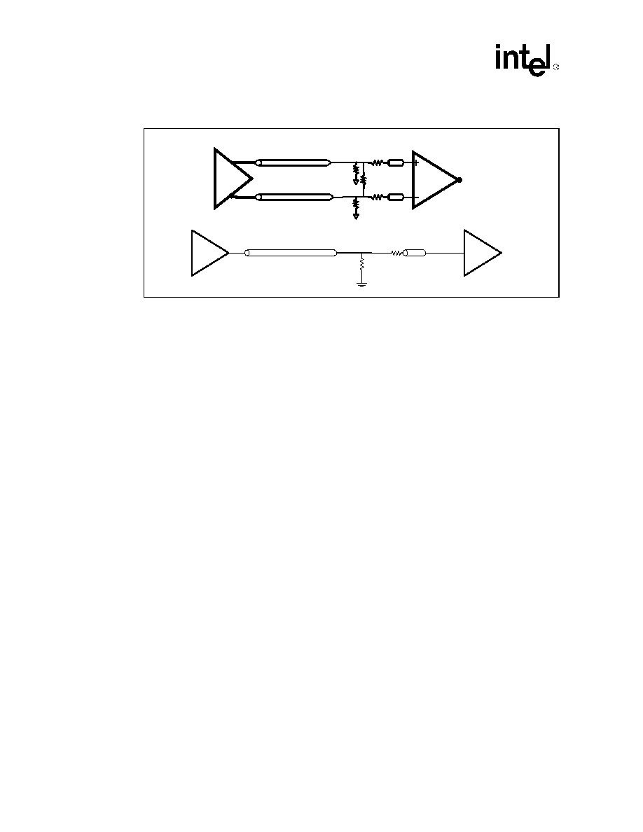
Figure 5. Differential/Single-Ended Clocking Example
BCLK
BCLK#
Clock
Driver
Processor or
Chipset
Clock
Driver
BCLK
Processor
or Chipset
相关PDF资料 |
PDF描述 |
|---|---|
| RK80532EC056512 | 2400 MHz, MICROPROCESSOR, CPGA604 |
| RK80532KE056512 | 32-BIT, 2400 MHz, MICROPROCESSOR, CPGA604 |
| BX80532KE3060D | 3060 MHz, MICROPROCESSOR, XMA |
| BX80532KE2400DU | 2400 MHz, MICROPROCESSOR, XMA604 |
| RK80532PG072512 | 2800 MHz, MICROPROCESSOR, PGA478 |
相关代理商/技术参数 |
参数描述 |
|---|---|
| RK80530KZ017512S L5XL | 制造商:Intel 功能描述:32BIT MPU 80530KZ017512 1.40G |
| RK80530KZ017512S L6BY | 制造商:Intel 功能描述:MPU Pentium 制造商:Intel 功能描述:MPU Pentium? III Processor-S 64-Bit 0.13um 1.4GHz 370-Pin FCPGA2 |
| RK80530PZ001256 | 制造商:未知厂家 制造商全称:未知厂家 功能描述:Microprocessor |
| RK80530PZ006256 | 制造商:未知厂家 制造商全称:未知厂家 功能描述:Microprocessor |
| RK80530PZ009256 | 制造商:Rochester Electronics LLC 功能描述:PIII 1.2G 256 ON DIE CACHE FC-PGA2 - Bulk |
发布紧急采购,3分钟左右您将得到回复。