- 您现在的位置:买卖IC网 > PDF目录69324 > S1C17554B00E10H 16-BIT, FLASH, 24 MHz, RISC MICROCONTROLLER, PBGA48 PDF资料下载
参数资料
| 型号: | S1C17554B00E10H |
| 元件分类: | 微控制器/微处理器 |
| 英文描述: | 16-BIT, FLASH, 24 MHz, RISC MICROCONTROLLER, PBGA48 |
| 封装: | 3.137 X 3.137 MM, 0.72 MM HEIGHT, 0.40 MM PITCH, WCSP-48 |
| 文件页数: | 246/318页 |
| 文件大小: | 2643K |
| 代理商: | S1C17554B00E10H |
第1页第2页第3页第4页第5页第6页第7页第8页第9页第10页第11页第12页第13页第14页第15页第16页第17页第18页第19页第20页第21页第22页第23页第24页第25页第26页第27页第28页第29页第30页第31页第32页第33页第34页第35页第36页第37页第38页第39页第40页第41页第42页第43页第44页第45页第46页第47页第48页第49页第50页第51页第52页第53页第54页第55页第56页第57页第58页第59页第60页第61页第62页第63页第64页第65页第66页第67页第68页第69页第70页第71页第72页第73页第74页第75页第76页第77页第78页第79页第80页第81页第82页第83页第84页第85页第86页第87页第88页第89页第90页第91页第92页第93页第94页第95页第96页第97页第98页第99页第100页第101页第102页第103页第104页第105页第106页第107页第108页第109页第110页第111页第112页第113页第114页第115页第116页第117页第118页第119页第120页第121页第122页第123页第124页第125页第126页第127页第128页第129页第130页第131页第132页第133页第134页第135页第136页第137页第138页第139页第140页第141页第142页第143页第144页第145页第146页第147页第148页第149页第150页第151页第152页第153页第154页第155页第156页第157页第158页第159页第160页第161页第162页第163页第164页第165页第166页第167页第168页第169页第170页第171页第172页第173页第174页第175页第176页第177页第178页第179页第180页第181页第182页第183页第184页第185页第186页第187页第188页第189页第190页第191页第192页第193页第194页第195页第196页第197页第198页第199页第200页第201页第202页第203页第204页第205页第206页第207页第208页第209页第210页第211页第212页第213页第214页第215页第216页第217页第218页第219页第220页第221页第222页第223页第224页第225页第226页第227页第228页第229页第230页第231页第232页第233页第234页第235页第236页第237页第238页第239页第240页第241页第242页第243页第244页第245页当前第246页第247页第248页第249页第250页第251页第252页第253页第254页第255页第256页第257页第258页第259页第260页第261页第262页第263页第264页第265页第266页第267页第268页第269页第270页第271页第272页第273页第274页第275页第276页第277页第278页第279页第280页第281页第282页第283页第284页第285页第286页第287页第288页第289页第290页第291页第292页第293页第294页第295页第296页第297页第298页第299页第300页第301页第302页第303页第304页第305页第306页第307页第308页第309页第310页第311页第312页第313页第314页第315页第316页第317页第318页
3 MEMORY MAP, BUS CONTROL
3-2
Seiko Epson Corporation
S1C17554/564 TECHNICAL MANUAL
1.1 Number of Bus Accesses
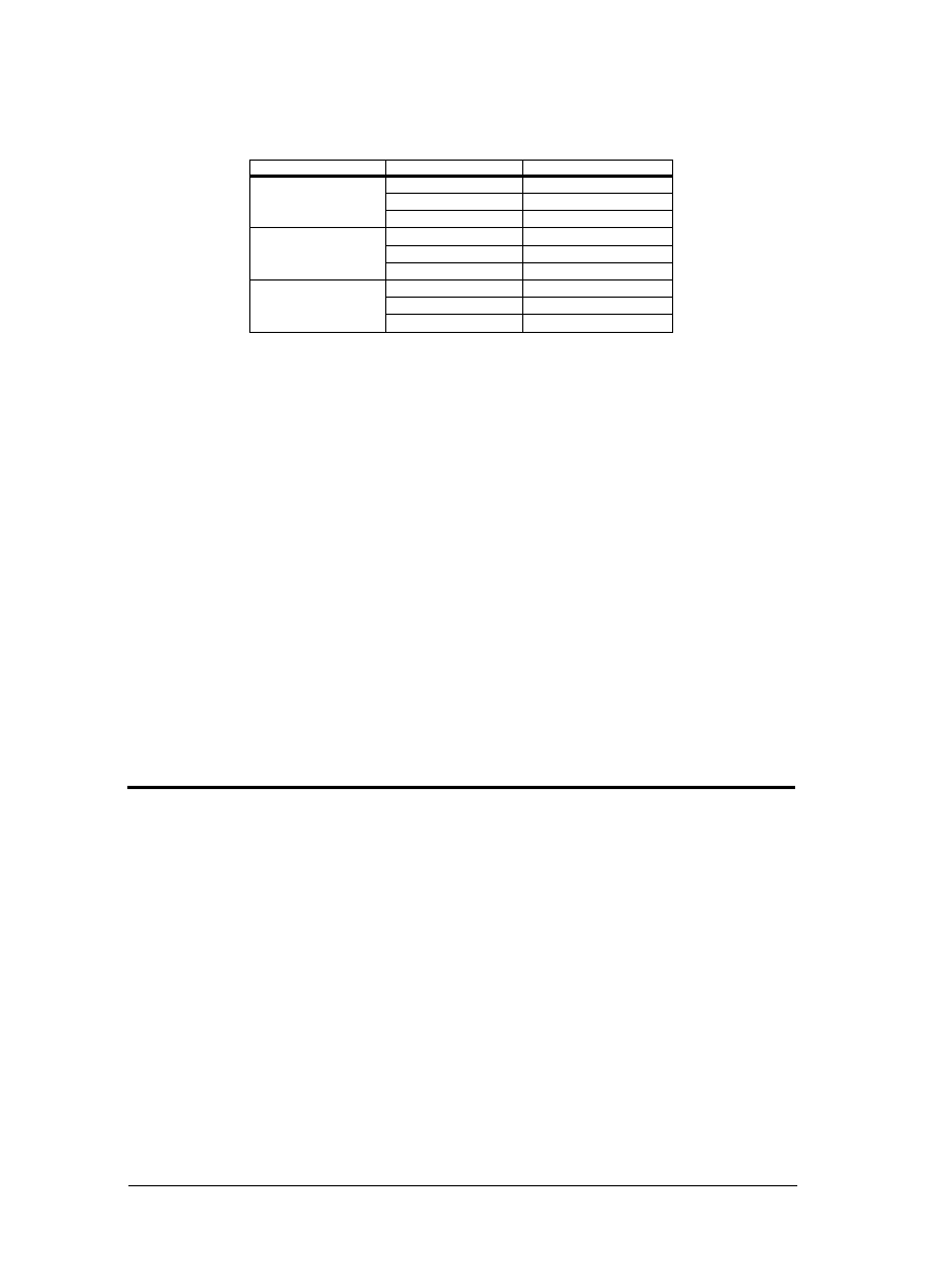
Table 3.
Device size
CPU access size
Number of bus accesses
8 bits
1
16 bits
2
32 bits*
4
16 bits
8 bits
1
16 bits
1
32 bits*
2
32 bits
8 bits
1
16 bits
1
32 bits*
1
* Handling the eight high-order bits during 32-bit accesses
The size of the S1C17 Core general-purpose registers is 24 bits.
During writing, the eight high-order bits are written as 0. During reading from a memory, the eight high-order
bits are ignored. However, the stack operation in an interrupt handling reads/writes 32-bit data that consists of the
PSR value as the high-order 8 bits and the return address as the low order 24 bits.
For more information, refer to the “S1C17 Core Manual.”
Restrictions on Access Size
3.1.1
The peripheral modules can be accessed with an 8-bit, 16-bit, or 32-bit instruction. However, reading for an unnec-
essary register may change the peripheral module status and it may cause a problem. Therefore, use the appropriate
instructions according to the device size.
Restrictions on Instruction Execution Cycles
3.1.2
An instruction fetch and a data access are not performed simultaneously under one of the conditions listed below.
This prolongs the instruction fetch cycle for the number of data area bus cycles.
When the S1C17554/564 executes the instruction stored in the Flash area and accesses data in the Flash area
When the S1C17554/564 executes the instruction stored in the internal RAM area and accesses data in the inter-
nal RAM area
Flash Area
3.2
Embedded Flash Memory
3.2.1
The 128K-byte area from address 0x8000 to address 0x27fff contains a Flash memory (4K bytes
× 32 sectors) for
storing application programs and data. Address 0x8000 is defined as the vector table base address, therefore a vec-
tor table (see “Vector Table” in the “Interrupt Controller (ITC)” chapter) must be placed from the beginning of the
area. The vector table base address can be modified with the MISC_TTBRL/MISC_TTBRH registers.
Flash Programming
3.2.2
The S1C17554/564 supports on-board programming of the Flash memory, it makes it possible to program the Flash
memory with the application programs/data by using the debugger through an ICDmini. The Flash memory sup-
ports sector erase method.
For the Flash programming using the debugger, see the “S5U1C17001C Manual” included in the S1C17 Family
C Compiler Package. For the self-programming controlled by the user program, see the “Self-Programming (FLS)
Application Notes” for the S1C17554/564.
相关PDF资料 |
PDF描述 |
|---|---|
| S1C17554B00E10M | 16-BIT, FLASH, 24 MHz, RISC MICROCONTROLLER, PBGA48 |
| S1C17554B00E10P | 16-BIT, FLASH, 24 MHz, RISC MICROCONTROLLER, PBGA48 |
| S1C17554B00E10R | 16-BIT, FLASH, 24 MHz, RISC MICROCONTROLLER, PBGA48 |
| S1C17554D00E10E | 16-BIT, FLASH, 24 MHz, RISC MICROCONTROLLER, UUC |
| S1C17554D00E10F | 16-BIT, FLASH, 24 MHz, RISC MICROCONTROLLER, UUC |
相关代理商/技术参数 |
参数描述 |
|---|---|
| S1C17555 | 制造商:EPSON 制造商全称:EPSON 功能描述:16-bit Single Chip Microcontroller |
| S1C17564 | 制造商:EPSON 制造商全称:EPSON 功能描述:16-bit Single Chip Microcontroller |
| S1C17564D111000 | 制造商:Epson Electronics America Inc 功能描述:16-bit, 128KB Flash (OSC3 = Ceramic) |
| S1C17564F111100 | 功能描述:显示驱动器和控制器 16-bit, 128KB Flash RoHS:否 制造商:Panasonic Electronic Components 工作电源电压:2.7 V to 5.5 V 最大工作温度: 安装风格:SMD/SMT 封装 / 箱体:QFN-44 封装:Reel |
| S1C17565 | 制造商:EPSON 制造商全称:EPSON 功能描述:16-bit Single Chip Microcontroller |
发布紧急采购,3分钟左右您将得到回复。