- 您现在的位置:买卖IC网 > PDF目录136617 > S1C17554B00E10L 16-BIT, FLASH, 24 MHz, RISC MICROCONTROLLER, PBGA48 PDF资料下载
参数资料
| 型号: | S1C17554B00E10L |
| 元件分类: | 微控制器/微处理器 |
| 英文描述: | 16-BIT, FLASH, 24 MHz, RISC MICROCONTROLLER, PBGA48 |
| 封装: | 3.137 X 3.137 MM, 0.72 MM HEIGHT, 0.40 MM PITCH, WCSP-48 |
| 文件页数: | 274/318页 |
| 文件大小: | 2643K |
| 代理商: | S1C17554B00E10L |
第1页第2页第3页第4页第5页第6页第7页第8页第9页第10页第11页第12页第13页第14页第15页第16页第17页第18页第19页第20页第21页第22页第23页第24页第25页第26页第27页第28页第29页第30页第31页第32页第33页第34页第35页第36页第37页第38页第39页第40页第41页第42页第43页第44页第45页第46页第47页第48页第49页第50页第51页第52页第53页第54页第55页第56页第57页第58页第59页第60页第61页第62页第63页第64页第65页第66页第67页第68页第69页第70页第71页第72页第73页第74页第75页第76页第77页第78页第79页第80页第81页第82页第83页第84页第85页第86页第87页第88页第89页第90页第91页第92页第93页第94页第95页第96页第97页第98页第99页第100页第101页第102页第103页第104页第105页第106页第107页第108页第109页第110页第111页第112页第113页第114页第115页第116页第117页第118页第119页第120页第121页第122页第123页第124页第125页第126页第127页第128页第129页第130页第131页第132页第133页第134页第135页第136页第137页第138页第139页第140页第141页第142页第143页第144页第145页第146页第147页第148页第149页第150页第151页第152页第153页第154页第155页第156页第157页第158页第159页第160页第161页第162页第163页第164页第165页第166页第167页第168页第169页第170页第171页第172页第173页第174页第175页第176页第177页第178页第179页第180页第181页第182页第183页第184页第185页第186页第187页第188页第189页第190页第191页第192页第193页第194页第195页第196页第197页第198页第199页第200页第201页第202页第203页第204页第205页第206页第207页第208页第209页第210页第211页第212页第213页第214页第215页第216页第217页第218页第219页第220页第221页第222页第223页第224页第225页第226页第227页第228页第229页第230页第231页第232页第233页第234页第235页第236页第237页第238页第239页第240页第241页第242页第243页第244页第245页第246页第247页第248页第249页第250页第251页第252页第253页第254页第255页第256页第257页第258页第259页第260页第261页第262页第263页第264页第265页第266页第267页第268页第269页第270页第271页第272页第273页当前第274页第275页第276页第277页第278页第279页第280页第281页第282页第283页第284页第285页第286页第287页第288页第289页第290页第291页第292页第293页第294页第295页第296页第297页第298页第299页第300页第301页第302页第303页第304页第305页第306页第307页第308页第309页第310页第311页第312页第313页第314页第315页第316页第317页第318页
7 CLOCK GENERATOR (CLG)
S1C17554/564 TECHNICAL MANUAL
Seiko Epson Corporation
7-11
D[1:0]
CLKSRC[1:0]: System Clock Source Select Bits
Selects the system clock source.
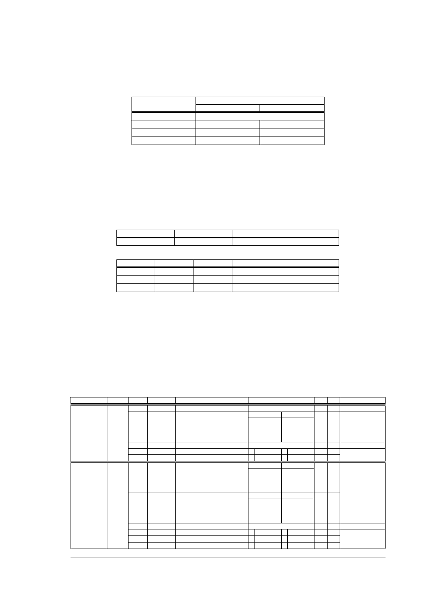
8.2 System Clock Selection
Table 7.
CLKSRC[1:0]
System clock source
S1C17554
S1C17564
0x3
Reserved
0x2
OSC3 (default)
OSC3
0x1
OSC1
0x0
Reserved
IOSC (default)
Select IOSC or OSC3 for normal (high-speed) operations. If no high-speed clock is required, OSC1 can
be set as the system clock and IOSC and OSC3 stopped to reduce current consumption.
Notes: The oscillator to be used as the system clock source must be operated before switching
the system clock. Otherwise, the CLG will not switch the system clock source, even if CLK-
SRC[1:0] is written to, and the CLKSRC[1:0] value will remain unchanged.
The tables below list the combinations of clock operating status and register settings en-
abling system clock selection.
8.3 System Clock Switching Conditions (S1C17554)
Table 7.
OSC3EN
OSC1EN
System clock
1
OSC3 or OSC1
8.4 System Clock Switching Conditions (S1C17564)
Table 7.
IOSCEN
OSC3EN
OSC1EN
System clock
1
IOSC, OSC3, or OSC1
1
0
1
IOSC or OSC1
0
1
OSC3 or OSC1
The oscillator circuit selected as the system clock source cannot be turned off.
Continuous write/read access to CLKSRC[1:0] is prohibited. At least one instruction unre-
lated to CLKSRC[1:0] access must be inserted between the write and read instructions.
When SLEEP mode is canceled in the S1C17564, the IOSC oscillator circuit is turned on
(IOSCEN = 1) and is used as the system clock source (CLKSRC[1:0] = 0x0) regardless of
the system clock configured before the chip entered SLEEP mode.
Canceling HALT mode does not change the clock status configured before the chip entered
HALT mode.
Oscillation Control Register (CLG_CTL)
Register name Address
Bit
Name
Function
Setting
Init. R/W
Remarks
Oscillation
Control Register
(CLG_CTL)
S1C17554
0x5061
(8 bits)
D7–6 –
reserved
–
0 when being read.
D5–4 OSC3WT[1:0] OSC3 wait cycle select
OSC3WT[1:0]
Wait cycle
0x0 R/W
0x3
0x2
0x1
0x0
128 cycles
256 cycles
512 cycles
1024 cycles
D3–2 –
reserved
–
0 when being read.
D1
OSC1EN
OSC1 enable
1 Enable
0 Disable
0
R/W
D0
OSC3EN
OSC3 enable
1 Enable
0 Disable
1
R/W
Oscillation
Control Register
(CLG_CTL)
S1C17564
0x5061
(8 bits)
D7–6 IOSCWT[1:0] IOSC wait cycle select
IOSCWT[1:0]
Wait cycle
0x0 R/W
0x3
0x2
0x1
0x0
8 cycles
16 cycles
32 cycles
64 cycles
D5–4 OSC3WT[1:0] OSC3 wait cycle select
OSC3WT[1:0]
Wait cycle
0x0 R/W
0x3
0x2
0x1
0x0
128 cycles
256 cycles
512 cycles
1024 cycles
D3
–
reserved
–
0 when being read.
D2
IOSCEN
IOSC enable
1 Enable
0 Disable
1
R/W
D1
OSC1EN
OSC1 enable
1 Enable
0 Disable
0
R/W
D0
OSC3EN
OSC3 enable
1 Enable
0 Disable
0
R/W
相关PDF资料 |
PDF描述 |
|---|---|
| S1C17554D00E10H | 16-BIT, FLASH, 24 MHz, RISC MICROCONTROLLER, UUC |
| S1C17554F00E10P | 16-BIT, FLASH, 24 MHz, RISC MICROCONTROLLER, PQFP64 |
| S1C17564D00E199 | 16-BIT, FLASH, 24 MHz, RISC MICROCONTROLLER, UUC |
| S1C17651B00E199 | 16-BIT, FLASH, 2 MHz, RISC MICROCONTROLLER, PBGA |
| SPC563M54L3COBR | 32-BIT, FLASH, 64 MHz, MICROCONTROLLER, PQFP100 |
相关代理商/技术参数 |
参数描述 |
|---|---|
| S1C17555 | 制造商:EPSON 制造商全称:EPSON 功能描述:16-bit Single Chip Microcontroller |
| S1C17564 | 制造商:EPSON 制造商全称:EPSON 功能描述:16-bit Single Chip Microcontroller |
| S1C17564D111000 | 制造商:Epson Electronics America Inc 功能描述:16-bit, 128KB Flash (OSC3 = Ceramic) |
| S1C17564F111100 | 功能描述:显示驱动器和控制器 16-bit, 128KB Flash RoHS:否 制造商:Panasonic Electronic Components 工作电源电压:2.7 V to 5.5 V 最大工作温度: 安装风格:SMD/SMT 封装 / 箱体:QFN-44 封装:Reel |
| S1C17565 | 制造商:EPSON 制造商全称:EPSON 功能描述:16-bit Single Chip Microcontroller |
发布紧急采购,3分钟左右您将得到回复。