- 您现在的位置:买卖IC网 > PDF目录368612 > S5N8947 (SAMSUNG SEMICONDUCTOR CO. LTD.) MCU for ADSL/Cable Modem PDF资料下载
参数资料
| 型号: | S5N8947 |
| 厂商: | SAMSUNG SEMICONDUCTOR CO. LTD. |
| 英文描述: | MCU for ADSL/Cable Modem |
| 中文描述: | 单片机为ADSL / Cable Modem的 |
| 文件页数: | 22/49页 |
| 文件大小: | 407K |
| 代理商: | S5N8947 |
第1页第2页第3页第4页第5页第6页第7页第8页第9页第10页第11页第12页第13页第14页第15页第16页第17页第18页第19页第20页第21页当前第22页第23页第24页第25页第26页第27页第28页第29页第30页第31页第32页第33页第34页第35页第36页第37页第38页第39页第40页第41页第42页第43页第44页第45页第46页第47页第48页第49页
S5N8947 (ADSL/Cable Modem MCU)
ELECTRONICS
MagIC Team
Page : 22
SAMSUNG ELECTRONICS
l
Four external I/O banks are defined in a continuous address space. A programmer can only set the
base pointer for external I/O bank 0. The start address of external I/O bank 1 is then calculated as the
external I/O bank 0 start address +16 K. Similary, the start address for external I/O bank 2 is the
external I/O bank 0 start address + 32 K, and the start address for external I/O bank 3 is the external
I/O bank 0 start address + 48 K. Therefore, the total consecutive addressable space of the four
external banks is defined as the start address of external I/O bank 0 + 64 K bytes.
l
Within the addressable space, the start address of each I/O bank is not fixed. You can use bank
control registers to assign a specific bank start address by setting the bank’s base pointer. The address
resolution is 64 K bytes. The bank’s start address is defined as “base pointer << 16” and the bank’s
end address (except for external I/O banks) is “next pointer << 16 – 1”.
After a power-on or system reset, all bank address pointer registers are initialized to their default
values. In this means that a system reset automatically defines ROM bank 0 as a 32-Mbyte space with a
start address of zero. This means that, except for ROM bank 0, all banks are undefined following a system
startup.
The reset value for the next pointer and base pointer of ROM bank 0 are 0x200 and 0x000,
respectively. This means that a system reset automatically defines ROM bank 0 as a 32-Mbyte space with a
start address of zero. This initial definition of ROM bank 0 lets the system power-on or reset operation
pass control to the user-supplied boot code that is stored in external ROM. (This code is located at address
0 in the system memory map.) When the boot code (i.e. ROM program) executes, it performs various
system initialization tasks and reconfigures the system memory map according to the application’s actual
external memory and device configuration.
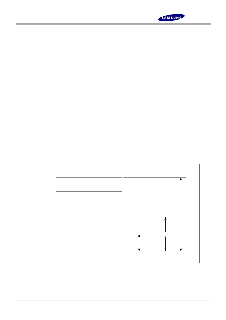
The initial system memory map following system startup is shown in following :
ROM/SRAM/FLASH
Bank 0 Area
(Accessible)
Undefined Area
Special Function
Registers
4 M Address[21:0]
ROM/SRAM/FLASH
Bank 0 Area
(Accessible)
32 M
64 M Bytes
SA[25:0]
0x0000000
0x2000000
0x3FF0000
0x3FFFFFF
Figure 5 Initial system memory map (After reset)
相关PDF资料 |
PDF描述 |
|---|---|
| S5N8947X | MCU for ADSL/Cable Modem |
| S5N8950 | G.dmt ADSL Transceiver for CO and CPE |
| S5N8951 | G.dmt ADSL Analog Front End IC |
| S5N8951X | G.dmt ADSL Analog Front End IC |
| S5N8952 | ADSL Transceiver for NIC |
相关代理商/技术参数 |
参数描述 |
|---|---|
| S5N8947X | 制造商:SAMSUNG 制造商全称:Samsung semiconductor 功能描述:MCU for ADSL/Cable Modem |
| S5N8950 | 制造商:SAMSUNG 制造商全称:Samsung semiconductor 功能描述:G.dmt ADSL Transceiver for CO and CPE |
| S5N8951 | 制造商:SAMSUNG 制造商全称:Samsung semiconductor 功能描述:G.dmt ADSL Analog Front End IC |
| S5N8951X | 制造商:SAMSUNG 制造商全称:Samsung semiconductor 功能描述:G.dmt ADSL Analog Front End IC |
| S5N8952 | 制造商:SAMSUNG 制造商全称:Samsung semiconductor 功能描述:ADSL Transceiver for NIC |
发布紧急采购,3分钟左右您将得到回复。