- 您现在的位置:买卖IC网 > PDF目录98082 > SL28505ALC PROC SPECIFIC CLOCK GENERATOR, QCC64 PDF资料下载
参数资料
| 型号: | SL28505ALC |
| 元件分类: | 时钟产生/分配 |
| 英文描述: | PROC SPECIFIC CLOCK GENERATOR, QCC64 |
| 封装: | 9 X 9 MM, 0.50 MM PITCH, ROHS COMPLIANT, QFN-64 |
| 文件页数: | 6/28页 |
| 文件大小: | 312K |
| 代理商: | SL28505ALC |
第1页第2页第3页第4页第5页当前第6页第7页第8页第9页第10页第11页第12页第13页第14页第15页第16页第17页第18页第19页第20页第21页第22页第23页第24页第25页第26页第27页第28页
SL28505
Rev 1.0 April 24, 2008
Page 14 of 28
Table 5. Crystal Recommendations
The SL28505 requires a parallel resonance crystal. Substi-
tuting a series resonance crystal causes the SL28505 to
operate at the wrong frequency and violate the ppm specifi-
cation. For most applications there is a 300-ppm frequency
shift between series and parallel crystals due to incorrect
loading.
Crystal Loading
Crystal loading plays a critical role in achieving low ppm perfor-
mance. To realize low ppm performance, the total capacitance
the crystal sees must be considered to calculate the appro-
priate capacitive loading (CL).
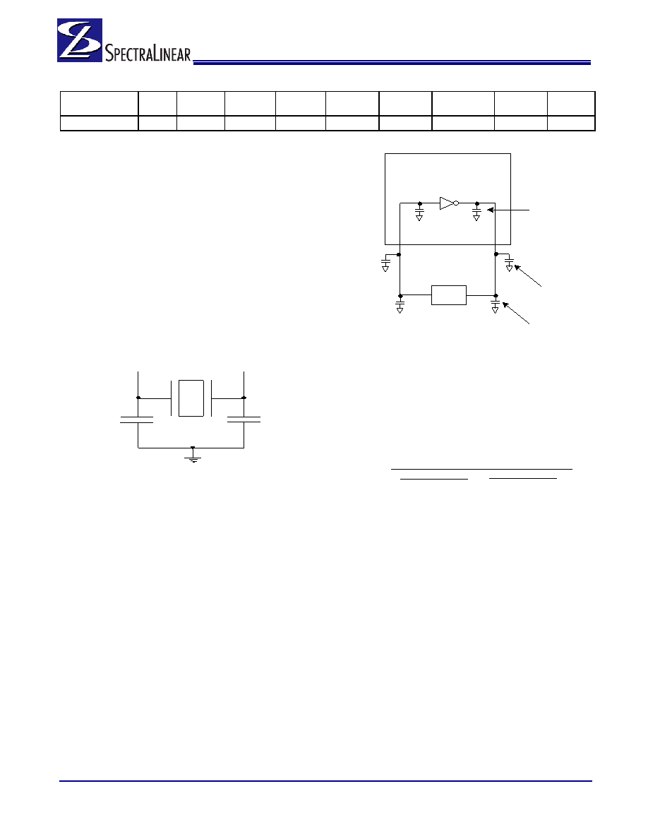
Figure 1 shows a typical crystal configuration using the two
trim capacitors. An important clarification for the following
discussion is that the trim capacitors are in series with the
crystal not parallel. The common misconception that load
capacitors are in parallel with the crystal and should be
approximately equal to the load capacitance of the crystal is
not true.
Calculating Load Capacitors
In addition to the standard external trim capacitors, trace
capacitance and pin capacitance must also be considered to
correctly calculate crystal loading. As mentioned previously,
the capacitance on each side of the crystal is in series with the
crystal. This means the total capacitance on each side of the
crystal must be twice the specified crystal load capacitance
(CL). While the capacitance on each side of the crystal is in
series with the crystal, trim capacitors (Ce1,Ce2) should be
calculated to provide equal capacitive loading on both sides.
Use the following formulas to calculate the trim capacitor
values for Ce1 and Ce2.
CL....................................................Crystal load capacitance
CLe......................................... Actual loading seen by crystal
using standard value trim capacitors
Ce..................................................... External trim capacitors
Cs .............................................. Stray capacitance (terraced)
Ci ...........................................................Internal capacitance
(lead frame, bond wires etc.)
Dial-A-Frequency (CPU & PCIEX)
This feature allows users to over-clock their systems by slowly
stepping up the CPU or SRC frequency. When the program-
mable output frequency feature is enabled, the CPU and SRC
frequencies are determined by the following equation:
Fcpu = G * N/M or Fcpu=G2 * N, where G2 = G/M.
‘N’ and ‘M’ are the values programmed in Programmable
Frequency Select N-Value Register and M-Value Register,
respectively. ‘G’ stands for the PLL Gear Constant, which is
determined by the programmed value of FS[E:A]. See
Frequency Table for the Gear Constant for each Frequency
selection. The PCI Express only allows user control of the N
register, the M value is fixed and documented in the Frequency
Select Table.
Frequency
(Fund)
Cut
Loading
Load Cap
Drive
(max.)
Shunt Cap
(max.)
Motional
(max.)
Tolerance
(max.)
Stability
(max.)
Aging
(max.)
14.31818 MHz
AT
Parallel
20 pF
0.1 mW
5 pF
0.016 pF
35 ppm
30 ppm
5 ppm
Figure 1. Crystal Capacitive Clarification
XTAL
Ce2
Ce1
Cs1
Cs2
X1
X2
Ci1
Ci2
Clock Chip
Trace
2.8 pF
Trim
33 pF
Pin
3 to 6p
Figure 2. Crystal Loading Example
Load Capacitance (each side)
Total Capacitance (as seen by the crystal)
Ce = 2 * CL – (Cs + Ci)
Ce1 + Cs1 + Ci1
1
+
Ce2 + Cs2 + Ci2
1
(
)
1
=
CLe
相关PDF资料 |
PDF描述 |
|---|---|
| SL28506BZC-2T | 400 MHz, PROC SPECIFIC CLOCK GENERATOR, PDSO56 |
| SL28506BOC-2 | PROC SPECIFIC CLOCK GENERATOR, PDSO56 |
| SL28506BZIT | 400 MHz, PROC SPECIFIC CLOCK GENERATOR, PDSO64 |
| SL28548ALC-2T | PROC SPECIFIC CLOCK GENERATOR, QCC64 |
| SL28610BLC | 100 MHz, PROC SPECIFIC CLOCK GENERATOR, QCC48 |
相关代理商/技术参数 |
参数描述 |
|---|---|
| SL28506BZC | 功能描述:时钟发生器及支持产品 CK505 v1.1 PCIe Gen2 RoHS:否 制造商:Silicon Labs 类型:Clock Generators 最大输入频率:14.318 MHz 最大输出频率:166 MHz 输出端数量:16 占空比 - 最大:55 % 工作电源电压:3.3 V 工作电源电流:1 mA 最大工作温度:+ 85 C 安装风格:SMD/SMT 封装 / 箱体:QFN-56 |
| SL28506BZC-2 | 功能描述:时钟发生器及支持产品 CK505 v1.1 PCIe Gen2 RoHS:否 制造商:Silicon Labs 类型:Clock Generators 最大输入频率:14.318 MHz 最大输出频率:166 MHz 输出端数量:16 占空比 - 最大:55 % 工作电源电压:3.3 V 工作电源电流:1 mA 最大工作温度:+ 85 C 安装风格:SMD/SMT 封装 / 箱体:QFN-56 |
| SL28506BZC-2T | 功能描述:时钟发生器及支持产品 CK505 v1.1 PCIe Gen2 RoHS:否 制造商:Silicon Labs 类型:Clock Generators 最大输入频率:14.318 MHz 最大输出频率:166 MHz 输出端数量:16 占空比 - 最大:55 % 工作电源电压:3.3 V 工作电源电流:1 mA 最大工作温度:+ 85 C 安装风格:SMD/SMT 封装 / 箱体:QFN-56 |
| SL28506BZCT | 功能描述:时钟发生器及支持产品 CK505 v1.1 PCIe Gen2 RoHS:否 制造商:Silicon Labs 类型:Clock Generators 最大输入频率:14.318 MHz 最大输出频率:166 MHz 输出端数量:16 占空比 - 最大:55 % 工作电源电压:3.3 V 工作电源电流:1 mA 最大工作温度:+ 85 C 安装风格:SMD/SMT 封装 / 箱体:QFN-56 |
| SL28506BZI | 功能描述:时钟发生器及支持产品 CK505 v1.1 PCIe Gen2 RoHS:否 制造商:Silicon Labs 类型:Clock Generators 最大输入频率:14.318 MHz 最大输出频率:166 MHz 输出端数量:16 占空比 - 最大:55 % 工作电源电压:3.3 V 工作电源电流:1 mA 最大工作温度:+ 85 C 安装风格:SMD/SMT 封装 / 箱体:QFN-56 |
发布紧急采购,3分钟左右您将得到回复。