- 您现在的位置:买卖IC网 > PDF目录97069 > SN74CBV3857DWR (TEXAS INSTRUMENTS INC) CBV SERIES, 10-BIT DRIVER, TRUE OUTPUT, PDSO24 PDF资料下载
参数资料
| 型号: | SN74CBV3857DWR |
| 厂商: | TEXAS INSTRUMENTS INC |
| 元件分类: | 总线收发器 |
| 英文描述: | CBV SERIES, 10-BIT DRIVER, TRUE OUTPUT, PDSO24 |
| 封装: | SOP-24 |
| 文件页数: | 1/7页 |
| 文件大小: | 88K |
| 代理商: | SN74CBV3857DWR |
SN74CBV3857
2.5-V 10-BIT FET BUS SWITCH
FOR DDR DIMMS
DESIGN GOAL
SCDS086A – FEBRUARY 1999 – REVISED MAY L999
1
POST OFFICE BOX 655303
DALLAS, TEXAS 75265
D Designed to be Used With 2.5-V DDR DIMM
Applications
D Switch On-State Resistance is Designed to
Eliminate the Series Resistor to the
DDR SDRAM
D Internal 200- Pulldown n-Channel FET to
Ground on Port B
D Internal 50-k Pullup Resistor on
Output-Enable Input
D Enable Signal Is SSTL_2 Compatible
D Flow-Through Architecture Optimizes PCB
Layout
D Package Options Include Shrink
Small-Outline (DBQ), Thin Very
Small-Outline (DGV), Small-Outline (DW),
and Thin Shrink Small-Outline (PW)
Packages
description
The SN74CBV3857 10-bit FET bus switch is designed for 2.3-V to 2.7-V VCC.
When the output-enable (OE) input is low, the 10-bit bus switch is on and port A is connected to port B. When
OE is high, the switch is open, the high-impedance state exists between the two ports, and port B is pulled down
by a 200-
n-channel FET to ground.
The FET switch on-state resistance is designed to replace the series terminating resistor in the SSTL_2 signal
path (see Figure 1).
11
0
0.4
0.8
1.2
1.6
2.0
2.4
2.8
3.2
0
7
9
13
15
17
19
21
Weak
Strong
Nominal
VI – Volts
–
on
r
Figure 1. On-State Resistance Characteristics
PRODUCT
PREVIEW
PRODUCT PREVIEW information concerns products in the formative or
design phase of development. Characteristic data and other
specifications are design goals. Texas Instruments reserves the right to
change or discontinue these products without notice.
Copyright
1999, Texas Instruments Incorporated
DESIGN GOAL
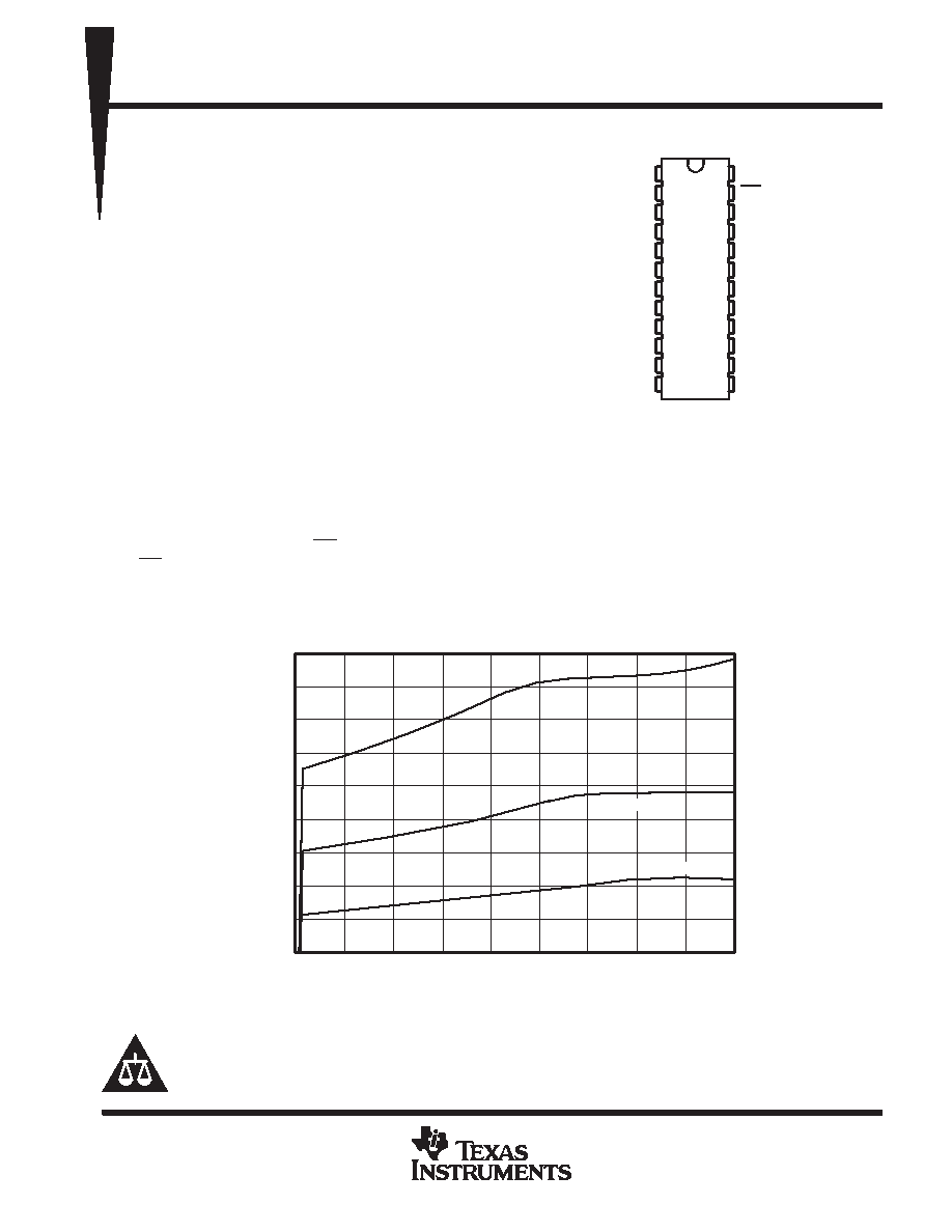
DBQ, DGV, DW, OR PW PACKAGE
(TOP VIEW)
VREF
A1
A2
A3
A4
A5
A6
A7
A8
A9
A10
GND
VCC
OE
B1
B2
B3
B4
B5
B6
B7
B8
B9
B10
1
2
3
4
5
6
7
8
9
10
11
12
24
23
22
21
20
19
18
17
16
15
14
13
Please be aware that an important notice concerning availability, standard warranty, and use in critical applications of
Texas Instruments semiconductor products and disclaimers thereto appears at the end of this data sheet.
相关PDF资料 |
PDF描述 |
|---|---|
| SN74F114N-10 | F/FAST SERIES, NEGATIVE EDGE TRIGGERED J-K FLIP-FLOP, COMPLEMENTARY OUTPUT, PDIP14 |
| SN74F151BNSRG4 | F/FAST SERIES, 8 LINE TO 1 LINE MULTIPLEXER, COMPLEMENTARY OUTPUT, PDSO16 |
| SN74F158ADR | F/FAST SERIES, QUAD 2 LINE TO 1 LINE MULTIPLEXER, INVERTED OUTPUT, PDSO16 |
| SN74F168N-10 | F/FAST SERIES, SYN POSITIVE EDGE TRIGGERED 4-BIT BIDIRECTIONAL DECADE COUNTER, PDIP16 |
| SNJ54F168J-00 | F/FAST SERIES, SYN POSITIVE EDGE TRIGGERED 4-BIT BIDIRECTIONAL DECADE COUNTER, CDIP16 |
相关代理商/技术参数 |
参数描述 |
|---|---|
| SN74CT540DW | 制造商:Texas Instruments 功能描述: |
| SN74F00D | 功能描述:逻辑门 Quad 2 Input RoHS:否 制造商:Texas Instruments 产品:OR 逻辑系列:LVC 栅极数量:2 线路数量(输入/输出):2 / 1 高电平输出电流:- 16 mA 低电平输出电流:16 mA 传播延迟时间:3.8 ns 电源电压-最大:5.5 V 电源电压-最小:1.65 V 最大工作温度:+ 125 C 安装风格:SMD/SMT 封装 / 箱体:DCU-8 封装:Reel |
| SN74F00D | 制造商:Texas Instruments 功能描述:GATE / INVERTER LOGIC IC |
| SN74F00DBR | 制造商:Rochester Electronics LLC 功能描述:- Bulk |
| SN74F00DE4 | 功能描述:逻辑门 Quad 2-input Positive-NAND gates RoHS:否 制造商:Texas Instruments 产品:OR 逻辑系列:LVC 栅极数量:2 线路数量(输入/输出):2 / 1 高电平输出电流:- 16 mA 低电平输出电流:16 mA 传播延迟时间:3.8 ns 电源电压-最大:5.5 V 电源电压-最小:1.65 V 最大工作温度:+ 125 C 安装风格:SMD/SMT 封装 / 箱体:DCU-8 封装:Reel |
发布紧急采购,3分钟左右您将得到回复。