- 您现在的位置:买卖IC网 > PDF目录365666 > SN74V3650-6PEU (Texas Instruments, Inc.) 3.3-V CMOS FIRST-IN, FIRST-OUT MEMORIES PDF资料下载
参数资料
| 型号: | SN74V3650-6PEU |
| 厂商: | Texas Instruments, Inc. |
| 英文描述: | 3.3-V CMOS FIRST-IN, FIRST-OUT MEMORIES |
| 中文描述: | 的3.3V的CMOS先入先出存储器 |
| 文件页数: | 4/50页 |
| 文件大小: | 729K |
| 代理商: | SN74V3650-6PEU |
第1页第2页第3页当前第4页第5页第6页第7页第8页第9页第10页第11页第12页第13页第14页第15页第16页第17页第18页第19页第20页第21页第22页第23页第24页第25页第26页第27页第28页第29页第30页第31页第32页第33页第34页第35页第36页第37页第38页第39页第40页第41页第42页第43页第44页第45页第46页第47页第48页第49页第50页
SN74V3640, SN74V3650, SN74V3660, SN74V3670, SN74V3680, SN74V3690
1024
×
36, 2048
×
36, 4096
×
36, 8192
×
36, 16384
×
36, 32768
×
36
3.3-V CMOS FIRST-IN, FIRST-OUT MEMORIES
SCAS668A
–
NOVEMBER 2001
–
REVISED MARCH 2003
4
POST OFFICE BOX 655303
DALLAS, TEXAS 75265
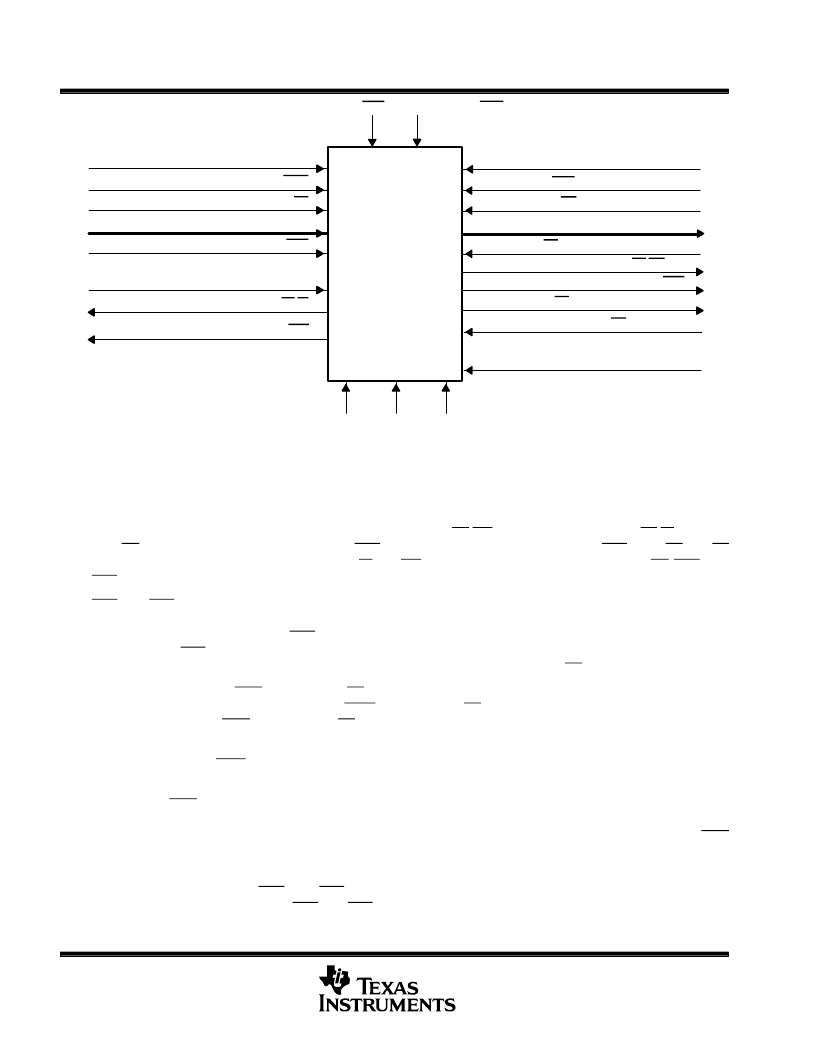
Bus
Matching
(BM)
SN74V3640
SN74V3650
SN74V3660
SN74V3670
SN74V3680
SN74V3690
Write Clock (WCLK)
Master Reset (MRS)
Partial Reset (PRS)
Read Clock (RCLK)
Write Enable (WEN)
Load (LD)
Serial Enable (SEN)
First-Word Fall-Through or Serial Input
(FWFT/SI)
Full Flag or Input Ready (FF/IR)
Programmable Almost-Full Flag (PAF)
(
×
36,
×
18,
×
9) Data In (D0
–
Dn)
Read Enable (REN)
Output Enable (OE)
(
×
36,
×
18,
×
9) Data Out (Q0
–
Qn)
Retransmit (RT)
Empty Flag or Output Ready (EF/OR)
Programmable Almost-Empty Flag (PAE)
Half-Full Flag (HF)
Big Endian/Little Endian (BE)
Interspersed/
Noninterspersed Parity (IP)
Input Width (IW)
Output Width (OW)
Figure 1. Single-Device-Configuration Signal Flow
description (continued)
These FIFOs have five flag pins: empty flag or output ready (EF/OR), full flag or input ready (FF/IR), half-full
flag (HF), programmable almost-empty flag (PAE), and programmable almost-full flag (PAF). The EF and FF
functions are selected in standard mode. The IR and OR functions are selected in FWFT mode. HF, PAE, and
PAF always are available for use, regardless of timing mode.
PAE and PAF can be programmed independently to switch at any point in memory. Programmable offsets
determine the flag-switching threshold and can be loaded by parallel or serial methods. Eight default offset
settings also are provided, so that PAE can be set to switch at a predefined number of locations from the empty
boundary. The PAF threshold also can be set at similar predefined values from the full boundary. The default
offset values are set during master reset by the state of the FSEL0, FSEL1, and LD.
For serial programming, SEN, together with LD, loads the offset registers via the serial input (SI) on each rising
edge of WCLK. For parallel programming, WEN, together with LD, loads the offset registers via Dn on each
rising edge of WCLK. REN, together with LD, can read the offsets in parallel from Qn on each rising edge of
RCLK, regardless of whether serial parallel offset loading has been selected.
During master reset (MRS), the read and write pointers are set to the first location of the FIFO. The FWFT pin
selects standard mode or FWFT mode.
Partial reset (PRS) also sets the read and write pointers to the first location of the memory. However, the timing
mode, programmable-flag programming method, and default or programmed offset settings existing before
partial reset remain unchanged. The flags are updated according to the timing mode and offsets in effect. PRS
is useful for resetting a device in mid-operation, when reprogramming programmable flags would be
undesirable.
Also, the timing modes of PAE and PAF outputs can be selected. Timing modes can be set as either
asynchronous or synchronous for PAE and PAF.
相关PDF资料 |
PDF描述 |
|---|---|
| SN74V3660-10PEU | 3.3-V CMOS FIRST-IN, FIRST-OUT MEMORIES |
| SN74V3660-15PEU | 3.3-V CMOS FIRST-IN, FIRST-OUT MEMORIES |
| SN74V3670-10PEU | 3.3-V CMOS FIRST-IN, FIRST-OUT MEMORIES |
| SN74V3670-15PEU | 3.3-V CMOS FIRST-IN, FIRST-OUT MEMORIES |
| SN74V3690-15PEU | 3.3-V CMOS FIRST-IN, FIRST-OUT MEMORIES |
相关代理商/技术参数 |
参数描述 |
|---|---|
| SN74V3650-7PEU | 功能描述:先进先出 2048 x 36 Synch 先进先出 Memory RoHS:否 制造商:IDT 电路数量: 数据总线宽度:18 bit 总线定向:Unidirectional 存储容量:4 Mbit 定时类型:Synchronous 组织:256 K x 18 最大时钟频率:100 MHz 访问时间:10 ns 电源电压-最大:3.6 V 电源电压-最小:6 V 最大工作电流:35 mA 最大工作温度:+ 85 C 封装 / 箱体:TQFP-80 封装: |
| SN74V3660-10PEU | 功能描述:先进先出 4096 x 36 Synch 先进先出 Memory RoHS:否 制造商:IDT 电路数量: 数据总线宽度:18 bit 总线定向:Unidirectional 存储容量:4 Mbit 定时类型:Synchronous 组织:256 K x 18 最大时钟频率:100 MHz 访问时间:10 ns 电源电压-最大:3.6 V 电源电压-最小:6 V 最大工作电流:35 mA 最大工作温度:+ 85 C 封装 / 箱体:TQFP-80 封装: |
| SN74V3660-15PEU | 功能描述:先进先出 4096 x 36 Synch 先进先出 Memory RoHS:否 制造商:IDT 电路数量: 数据总线宽度:18 bit 总线定向:Unidirectional 存储容量:4 Mbit 定时类型:Synchronous 组织:256 K x 18 最大时钟频率:100 MHz 访问时间:10 ns 电源电压-最大:3.6 V 电源电压-最小:6 V 最大工作电流:35 mA 最大工作温度:+ 85 C 封装 / 箱体:TQFP-80 封装: |
| SN74V3660-6PEU | 功能描述:先进先出 4096 x 36 Synch 先进先出 Memory RoHS:否 制造商:IDT 电路数量: 数据总线宽度:18 bit 总线定向:Unidirectional 存储容量:4 Mbit 定时类型:Synchronous 组织:256 K x 18 最大时钟频率:100 MHz 访问时间:10 ns 电源电压-最大:3.6 V 电源电压-最小:6 V 最大工作电流:35 mA 最大工作温度:+ 85 C 封装 / 箱体:TQFP-80 封装: |
| SN74V3660-7PEU | 功能描述:先进先出 4096 x 36 Synch 先进先出 Memory RoHS:否 制造商:IDT 电路数量: 数据总线宽度:18 bit 总线定向:Unidirectional 存储容量:4 Mbit 定时类型:Synchronous 组织:256 K x 18 最大时钟频率:100 MHz 访问时间:10 ns 电源电压-最大:3.6 V 电源电压-最小:6 V 最大工作电流:35 mA 最大工作温度:+ 85 C 封装 / 箱体:TQFP-80 封装: |
发布紧急采购,3分钟左右您将得到回复。