- 您现在的位置:买卖IC网 > PDF目录365666 > SN74V3650-6PEU (Texas Instruments, Inc.) 3.3-V CMOS FIRST-IN, FIRST-OUT MEMORIES PDF资料下载
参数资料
| 型号: | SN74V3650-6PEU |
| 厂商: | Texas Instruments, Inc. |
| 英文描述: | 3.3-V CMOS FIRST-IN, FIRST-OUT MEMORIES |
| 中文描述: | 的3.3V的CMOS先入先出存储器 |
| 文件页数: | 6/50页 |
| 文件大小: | 729K |
| 代理商: | SN74V3650-6PEU |
第1页第2页第3页第4页第5页当前第6页第7页第8页第9页第10页第11页第12页第13页第14页第15页第16页第17页第18页第19页第20页第21页第22页第23页第24页第25页第26页第27页第28页第29页第30页第31页第32页第33页第34页第35页第36页第37页第38页第39页第40页第41页第42页第43页第44页第45页第46页第47页第48页第49页第50页
SN74V3640, SN74V3650, SN74V3660, SN74V3670, SN74V3680, SN74V3690
1024
×
36, 2048
×
36, 4096
×
36, 8192
×
36, 16384
×
36, 32768
×
36
3.3-V CMOS FIRST-IN, FIRST-OUT MEMORIES
SCAS668A
–
NOVEMBER 2001
–
REVISED MARCH 2003
6
POST OFFICE BOX 655303
DALLAS, TEXAS 75265
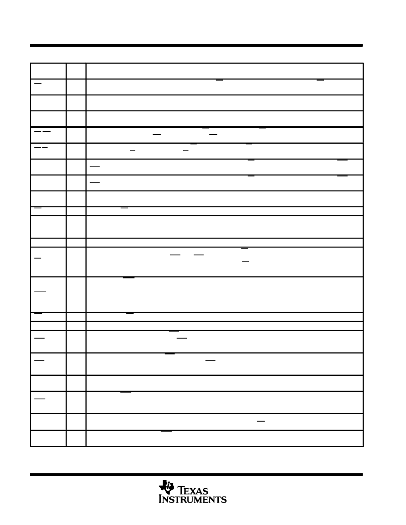
Terminal Functions
TERMINAL
NAME
I/O
DESCRIPTION
BE
I
Big endian/little endian. During master reset, a low on BE selects big-endian operation. A high on BE during master
reset selects little-endian format.
BM
I
Bus matching. BM works with IW and OW to select the bus sizes for both write and read ports (see Table 1 for bus-size
configuration).
D0
–
D36
I
Data inputs. Data inputs for a 36-, 18-, or 9-bit bus. When in 18- or 9-bit mode, the unused input pins are in a
don
’
t-care state.
EF/OR
O
Empty flag/output ready. In standard mode, the EF function is selected. EF indicates whether the FIFO memory is
empty. In FWFT mode, the OR function is selected. OR indicates whether there is valid data available at the outputs.
FF/IR
O
Full flag/input ready. In standard mode, the FF function is selected. FF indicates whether the FIFO memory is full. In
FWFT mode, the IR function is selected. IR indicates whether there is space available for writing to the FIFO memory.
FSEL0
I
Flag-select bit 0. During master reset, FSEL0, along with FSEL1 and LD, selects the default offset values for PAE and
PAF. Up to eight possible settings are available.
FSEL1
I
Flag-select bit 1. During master reset, FSEL1, along with FSEL0 and LD, selects the default offset values for PAE and
PAF. Up to eight possible settings are available.
FWFT/SI
I
First-word fall-through/serial in. During master reset, FWFT/SI selects FWFT or standard mode. After master reset,
FWFT/SI functions as a serial input for loading offset registers.
HF
O
Half-full flag. HF indicates whether the FIFO memory is more or less than half full.
IP
I
Interspersed parity. During master reset, a low on IP selects noninterspersed-parity mode. A high selects
interspersed-parity mode. Interspersed-parity control has an effect only during parallel programming of the offset
registers. It does not effect data written to and read from the FIFO.
IW
I
Input width. IW, along with OW and BM, selects the bus width of the write port (see Table 1 for bus-size configuration).
LD
I
Load. This is a dual-purpose pin. During master reset, the state of LD, along with FSEL0 and FSEL1, determines one
of eight default offset values for PAE and PAF, along with the method by which these offset registers can be
programmed, parallel or serial (see Table 2). After master reset, LD enables writing to and reading from the offset
registers.
MRS
I
Master reset. MRS initializes the read and write pointers to zero and sets the output register to all zeroes. During
master reset, the FIFO is configured for either FWFT or standard mode, bus-matching configurations, one of eight
programmable-flag default settings, serial or parallel programming of the offset settings, big-endian/little-endian
format, zero-latency timing mode, interspersed parity, and synchronous versus asynchronous programmable-flag
timing modes.
OE
OW
I
Output enable. OE controls the output impedance of Qn.
I
Output width. OW, along with IW and BM, selects the bus width of the read port (see Table 1 for bus-size configuration).
PAE
O
Programmable almost-empty flag. PAE goes low if the number of words in the FIFO memory is less than offset n, which
is stored in the empty offset register. PAE goes high if the number of words in the FIFO memory is greater than, or
equal to, offset n.
PAF
O
Programmable almost-full flag. PAF goes high if the number of free locations in the FIFO memory is more than
offset m, which is stored in the full offset register. PAF goes low if the number of free locations in the FIFO memory
is less than, or equal to, m.
PFM
I
Programmable-flag mode. During master reset, a low on PFM selects asynchronous programmable-flag timing mode.
A high on PFM selects synchronous programmable-flag timing mode.
PRS
I
Partial reset. PRS initializes the read and write pointers to zero and sets the output register to all zeroes. During partial
reset, the existing mode (standard or FWFT), programming method (serial or parallel), and programmable-flag
settings are all retained.
Q0
–
Q35
O
Data outputs. Data outputs for a 36-, 18-, or 9-bit bus. When in 18- or 9-bit mode, the unused output pins are in a
don
’
t-care state. Outputs are not 5-V tolerant, regardless of the state of OE.
RCLK
I
Read clock. When enabled by REN, the rising edge of RCLK reads data from the FIFO memory and offsets from the
programmable registers.
Inputs should not change state after master reset.
相关PDF资料 |
PDF描述 |
|---|---|
| SN74V3660-10PEU | 3.3-V CMOS FIRST-IN, FIRST-OUT MEMORIES |
| SN74V3660-15PEU | 3.3-V CMOS FIRST-IN, FIRST-OUT MEMORIES |
| SN74V3670-10PEU | 3.3-V CMOS FIRST-IN, FIRST-OUT MEMORIES |
| SN74V3670-15PEU | 3.3-V CMOS FIRST-IN, FIRST-OUT MEMORIES |
| SN74V3690-15PEU | 3.3-V CMOS FIRST-IN, FIRST-OUT MEMORIES |
相关代理商/技术参数 |
参数描述 |
|---|---|
| SN74V3650-7PEU | 功能描述:先进先出 2048 x 36 Synch 先进先出 Memory RoHS:否 制造商:IDT 电路数量: 数据总线宽度:18 bit 总线定向:Unidirectional 存储容量:4 Mbit 定时类型:Synchronous 组织:256 K x 18 最大时钟频率:100 MHz 访问时间:10 ns 电源电压-最大:3.6 V 电源电压-最小:6 V 最大工作电流:35 mA 最大工作温度:+ 85 C 封装 / 箱体:TQFP-80 封装: |
| SN74V3660-10PEU | 功能描述:先进先出 4096 x 36 Synch 先进先出 Memory RoHS:否 制造商:IDT 电路数量: 数据总线宽度:18 bit 总线定向:Unidirectional 存储容量:4 Mbit 定时类型:Synchronous 组织:256 K x 18 最大时钟频率:100 MHz 访问时间:10 ns 电源电压-最大:3.6 V 电源电压-最小:6 V 最大工作电流:35 mA 最大工作温度:+ 85 C 封装 / 箱体:TQFP-80 封装: |
| SN74V3660-15PEU | 功能描述:先进先出 4096 x 36 Synch 先进先出 Memory RoHS:否 制造商:IDT 电路数量: 数据总线宽度:18 bit 总线定向:Unidirectional 存储容量:4 Mbit 定时类型:Synchronous 组织:256 K x 18 最大时钟频率:100 MHz 访问时间:10 ns 电源电压-最大:3.6 V 电源电压-最小:6 V 最大工作电流:35 mA 最大工作温度:+ 85 C 封装 / 箱体:TQFP-80 封装: |
| SN74V3660-6PEU | 功能描述:先进先出 4096 x 36 Synch 先进先出 Memory RoHS:否 制造商:IDT 电路数量: 数据总线宽度:18 bit 总线定向:Unidirectional 存储容量:4 Mbit 定时类型:Synchronous 组织:256 K x 18 最大时钟频率:100 MHz 访问时间:10 ns 电源电压-最大:3.6 V 电源电压-最小:6 V 最大工作电流:35 mA 最大工作温度:+ 85 C 封装 / 箱体:TQFP-80 封装: |
| SN74V3660-7PEU | 功能描述:先进先出 4096 x 36 Synch 先进先出 Memory RoHS:否 制造商:IDT 电路数量: 数据总线宽度:18 bit 总线定向:Unidirectional 存储容量:4 Mbit 定时类型:Synchronous 组织:256 K x 18 最大时钟频率:100 MHz 访问时间:10 ns 电源电压-最大:3.6 V 电源电压-最小:6 V 最大工作电流:35 mA 最大工作温度:+ 85 C 封装 / 箱体:TQFP-80 封装: |
发布紧急采购,3分钟左右您将得到回复。