- 您现在的位置:买卖IC网 > PDF目录69349 > ST62P15CB3 (STMICROELECTRONICS) MICROCONTROLLER, PDIP28 PDF资料下载
参数资料
| 型号: | ST62P15CB3 |
| 厂商: | STMICROELECTRONICS |
| 元件分类: | 微控制器/微处理器 |
| 英文描述: | MICROCONTROLLER, PDIP28 |
| 封装: | PLASTIC, DIP-28 |
| 文件页数: | 10/105页 |
| 文件大小: | 1412K |
| 代理商: | ST62P15CB3 |
第1页第2页第3页第4页第5页第6页第7页第8页第9页当前第10页第11页第12页第13页第14页第15页第16页第17页第18页第19页第20页第21页第22页第23页第24页第25页第26页第27页第28页第29页第30页第31页第32页第33页第34页第35页第36页第37页第38页第39页第40页第41页第42页第43页第44页第45页第46页第47页第48页第49页第50页第51页第52页第53页第54页第55页第56页第57页第58页第59页第60页第61页第62页第63页第64页第65页第66页第67页第68页第69页第70页第71页第72页第73页第74页第75页第76页第77页第78页第79页第80页第81页第82页第83页第84页第85页第86页第87页第88页第89页第90页第91页第92页第93页第94页第95页第96页第97页第98页第99页第100页第101页第102页第103页第104页第105页
ST6215C/ST6225C
12/105
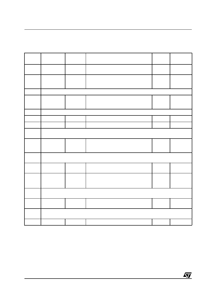
MEMORY MAP (Cont’d)
Table 2. Hardware Register Map
Legend:
x = undefined, R/W = Read/Write, Ro = Read-only Bit(s) in the register, Wo = Write-only Bit(s)
in the register.
Notes:
1. The contents of the I/O port DR registers are readable only in output configuration. In input configura-
tion, the values of the I/O pins are returned instead of the DR register contents.
2. The bits associated with unavailable pins must always be kept at their reset value.
3. Do not use single-bit instructions (SET, RES...) on Port Data Registers if any pin of the port is configured
in input mode (refer to Section 8 "I/O PORTS" on page 38 for more details).
Address
Block
Register
Label
Register Name
Reset
Status
Remarks
080h
to 083h
CPU
X,Y,V,W
X,Y index registers
V,W short direct registers
xxh
R/W
0C0h
0C1h
0C2h
I/O Ports
DRA 1) 2) 3)
DRB 1) 2) 3)
DRC 1) 2) 3)
Port A Data Register
Port B Data Register
Port C Data Register
00h
R/W
0C3h
Reserved (1 Byte)
0C4h
0C5h
0C6h
I/O Ports
DDRA 2)
DDRB 2)
DDRC 2)
Port A Direction Register
Port B Direction Register
Port C Direction Register
00h
R/W
0C7h
Reserved (1 Byte)
0C8h
CPU
IOR
Interrupt Option Register
xxh
Write-only
0C9h
ROM
DRWR
Data ROM Window register
xxh
Write-only
0CAh
0CBh
Reserved (2 Bytes)
0CCh
0CDh
0CEh
I/O Ports
ORA 2)
ORB 2)
ORC 2)
Port A Option Register
Port B Option Register
Port C Option Register
00h
R/W
0CFh
Reserved (1 byte)
0D0h
0D1h
ADC
ADR
ADCR
A/D Converter Data Register
A/D Converter Control Register
xxh
40h
Read-only
Ro/Wo
0D2h
0D3h
0D4h
Timer1
PSCR
TCR
TSCR
Timer 1 Prescaler Register
Timer 1 Counter Register
Timer 1 Status Control Register
7Fh
0FFh
00h
R/W
0D5h
to 0D7h
Reserved (3 Bytes)
0D8h
Watchdog
Timer
WDGR
Watchdog Register
0FEh
R/W
0D9h
to 0FEh
Reserved (38 Bytes)
0FFh
CPU
A
Accumulator
xxh
R/W
1
相关PDF资料 |
PDF描述 |
|---|---|
| ST6215CB3/CCC | MICROCONTROLLER, PDIP28 |
| ST62P15CM3 | MICROCONTROLLER, PDSO28 |
| ST62P15CN3 | MICROCONTROLLER, PDSO28 |
| ST6225CN3/CCC | MICROCONTROLLER, PDSO28 |
| ST62P30BM3/XXX | 8-BIT, MROM, 4 MHz, MICROCONTROLLER, PDSO28 |
相关代理商/技术参数 |
参数描述 |
|---|---|
| ST62P15CM6/AITTR | 制造商:STMicroelectronics 功能描述: |
| ST62P52C | 制造商:STMicroelectronics 功能描述: |
| ST62P62CM6/MOMTR | 制造商:STMicroelectronics 功能描述: |
| ST62P62CM6/MPITR | 制造商:STMicroelectronics 功能描述: |
| ST62P62CM6/MSATR | 制造商:STMicroelectronics 功能描述: |
发布紧急采购,3分钟左右您将得到回复。