- 您现在的位置:买卖IC网 > PDF目录69498 > TNY265PG (POWER INTEGRATIONS INC) 0.44 A SWITCHING REGULATOR, 140 kHz SWITCHING FREQ-MAX, PDIP7 PDF资料下载
参数资料
| 型号: | TNY265PG |
| 厂商: | POWER INTEGRATIONS INC |
| 元件分类: | 稳压器 |
| 英文描述: | 0.44 A SWITCHING REGULATOR, 140 kHz SWITCHING FREQ-MAX, PDIP7 |
| 封装: | 0.300 INCH, LEAD FREE, PLASTIC, MS-001-AB, DIP-8 |
| 文件页数: | 1/22页 |
| 文件大小: | 760K |
| 代理商: | TNY265PG |
www.powerint.com
February 2009
TNY263-268
TinySwitch-II Family
Enhanced, Energy Efficient, Low Power
Off-line Switcher
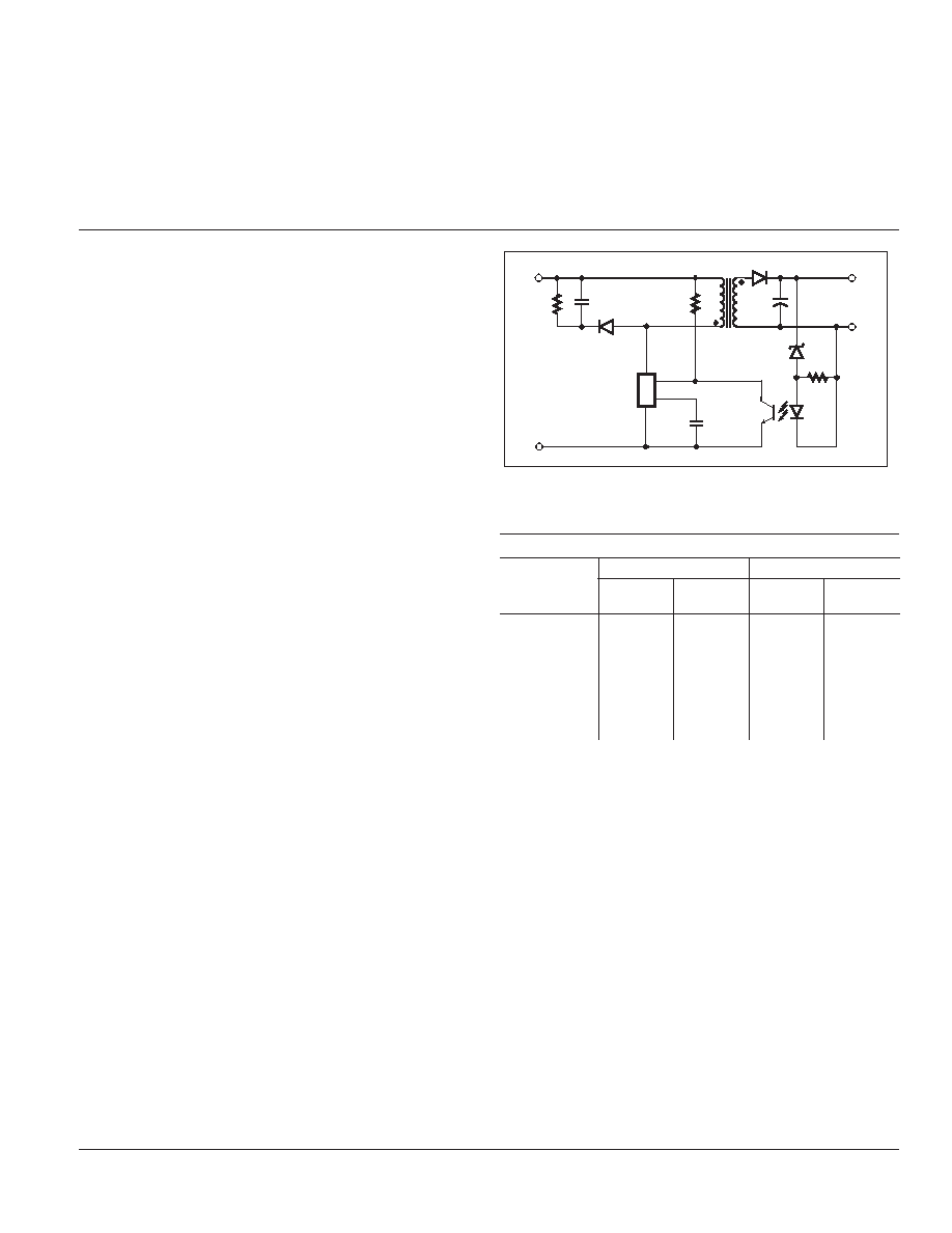
Figure 1.
Typical Standby Application.
Product Highlights
TinySwitch-II Features Reduce System Cost
Fully integrated auto-restart for short circuit and open loop fault
protection – saves external component costs
Built-in circuitry practically eliminates audible noise with ordinary
dip-varnished transformer
Programmable line undervoltage detect feature prevents power
on/off glitches – saves external components
Frequency jittering dramatically reduces EMI (~10 dB)
– minimizes EMI lter component costs
132 kHz operation reduces transformer size – allows use of
EF12.6 or EE13 cores for low cost and small size
Very tight tolerances and negligible temperature variation on key
parameters eases design and lowers cost
Lowest component count switcher solution
Expanded scalable device family for low system cost
Better Cost/Performance over RCC & Linears
Lower system cost than RCC, discrete PWM and other
integrated/hybrid solutions
Cost effective replacement for bulky regulated linears
Simple ON/OFF control – no loop compensation needed
No bias winding – simpler, lower cost transformer
Simple design practically eliminates rework in manufacturing
EcoSmart
– Extremely Energy Efcient
No load consumption <50 mW with bias winding and
<250 mW without bias winding at 265 VAC input
Meets California Energy Commission (CEC), Energy Star, and
EU requirements
Ideal for cell-phone charger and PC standby applications
High Performance at Low Cost
High voltage powered – ideal for charger applications
High bandwidth provides fast turn on with no overshoot
Current limit operation rejects line frequency ripple
Built-in current limit and thermal protection improves safety
Description
TinySwitch-II integrates a 700 V power MOSFET, oscillator, high
voltage switched current source, current limit and thermal
shutdown circuitry onto a monolithic device. The start-up and
operating power are derived directly from the voltage on the
DRAIN pin, eliminating the need for a bias winding and
associated circuitry. In addition, the TinySwitch-II devices
incorporate auto-restart, line undervoltage sense, and frequency
jittering. An innovative design minimizes audio frequency
components in the simple ON/OFF control scheme to practically
eliminate audible noise with standard taped/varnished
PI-2684-021809
Wide-Range
HV DC Input
D
S
EN/UV
BP
+
-
+
-
DC
Output
TinySwitch-II
Optional
UV Resistor
transformer construction. The fully integrated auto-restart circuit
safely limits output power during fault conditions such as output
short circuit or open loop, reducing component count and
secondary feedback circuitry cost. An optional line sense resistor
externally programs a line undervoltage threshold, which
eliminates power down glitches caused by the slow discharge of
input storage capacitors present in applications such as standby
supplies. The operating frequency of 132 kHz is jittered to
signicantly reduce both the quasi-peak and average EMI,
minimizing ltering cost.
Output Power Table
Product3
230 VAC ± 15%
85-265 VAC
Adapter1
Open
Frame2
Adapter1
Open
Frame2
TNY263 P/G
5 W
7.5 W
3.7 W
4.7 W
TNY264 P/G
5.5 W
9 W
4 W
6 W
TNY265 P/G
8.5 W
11 W
5.5 W
7.5 W
TNY266 P/G
10 W
15 W
6 W
9.5 W
TNY267 P/G
13 W
19 W
8 W
12 W
TNY268 P/G
16 W
23 W
10 W
15 W
Table 1.
Output Power Table.
Notes:
1. Minimum continuous power in a typical non-ventilated enclosed adapter
measured at 50 °C ambient.
2. Minimum practical continuous power in an open frame design with adequate
heat sinking, measured at 50 °C ambient (See Key Applications
Considerations).
3. Packages: P: DIP-8B, G: SMD-8B. Please see Part Ordering Information.
相关PDF资料 |
PDF描述 |
|---|---|
| TNY277PG | 0.481 A SWITCHING REGULATOR, PDIP7 |
| TNY279PG | 0.695 A SWITCHING REGULATOR, PDIP7 |
| TNY376GN | 0.496 A SWITCHING REGULATOR, 280 kHz SWITCHING FREQ-MAX, PDSO7 |
| TNY378GN-TL | 0.779 A SWITCHING REGULATOR, 280 kHz SWITCHING FREQ-MAX, PDSO7 |
| TNY379GN-TL | 0.921 A SWITCHING REGULATOR, 280 kHz SWITCHING FREQ-MAX, PDSO7 |
相关代理商/技术参数 |
参数描述 |
|---|---|
| TNY265PN | 功能描述:交流/直流开关转换器 7.5W 85-265 VAC 11W/230 VAC RoHS:否 制造商:STMicroelectronics 输出电压:800 V 输入/电源电压(最大值):23.5 V 输入/电源电压(最小值):11.5 V 开关频率:115 kHz 电源电流:1.6 mA 工作温度范围:- 40 C to + 150 C 安装风格:SMD/SMT 封装 / 箱体:SSO-10 封装:Reel |
| TNY265PN-TL | 制造商:POWERINT 制造商全称:Power Integrations, Inc. 功能描述:Enhanced, Energy Efficient, Low Power Off-line Switcher |
| TNY265PTL | 制造商:POWERINT 制造商全称:Power Integrations, Inc. 功能描述:Enhanced, Energy Efficient, Low Power Off-line Switcher |
| TNY266 | 制造商:POWERINT 制造商全称:Power Integrations, Inc. 功能描述:Generic PCB for DVD Player using TinySwitch-II |
| TNY266G | 功能描述:IC OFFLINE SWIT OTP OCP HV 8SMD RoHS:否 类别:集成电路 (IC) >> PMIC - AC-DC 转换器,离线开关 系列:TinySwitch®-II 标准包装:1 系列:FPS™ 输出隔离:隔离 频率范围:61kHz ~ 73kHz 输入电压:8 V ~ 26 V 输出电压:650V 功率(瓦特):12W 工作温度:-40°C ~ 115°C 封装/外壳:8-DIP(0.300",7.62mm) 供应商设备封装:8-MDIP 包装:Digi-Reel® 其它名称:FSL206MRBNFSDKR |
发布紧急采购,3分钟左右您将得到回复。