- 您现在的位置:买卖IC网 > PDF目录202172 > V59C1G01168QBLJ-25I (PROMOS TECHNOLOGIES INC) DDR DRAM, PBGA84 PDF资料下载
参数资料
| 型号: | V59C1G01168QBLJ-25I |
| 厂商: | PROMOS TECHNOLOGIES INC |
| 元件分类: | DRAM |
| 英文描述: | DDR DRAM, PBGA84 |
| 封装: | GREEN, FBGA-84 |
| 文件页数: | 15/82页 |
| 文件大小: | 995K |
| 代理商: | V59C1G01168QBLJ-25I |
第1页第2页第3页第4页第5页第6页第7页第8页第9页第10页第11页第12页第13页第14页当前第15页第16页第17页第18页第19页第20页第21页第22页第23页第24页第25页第26页第27页第28页第29页第30页第31页第32页第33页第34页第35页第36页第37页第38页第39页第40页第41页第42页第43页第44页第45页第46页第47页第48页第49页第50页第51页第52页第53页第54页第55页第56页第57页第58页第59页第60页第61页第62页第63页第64页第65页第66页第67页第68页第69页第70页第71页第72页第73页第74页第75页第76页第77页第78页第79页第80页第81页第82页
22
V59C1G01(408/808/168)QB Rev. 1.1 December 2008
ProMOS TECHNOLOGIES
V59C1G01(408/808/168)QB
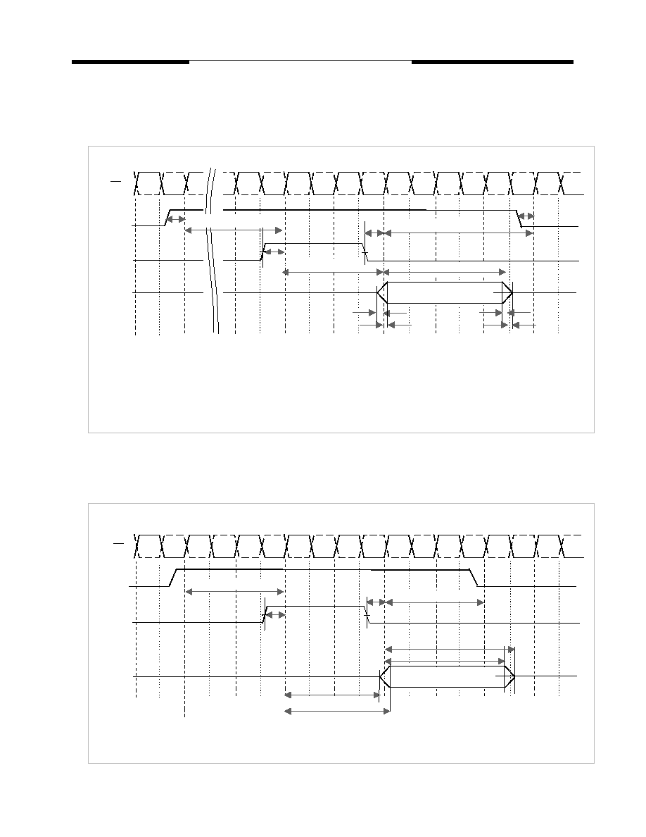
ODT Timing for Active / Standby (Idle) Mode and Standard Acti ve Power-Do wn Mode
ODT Timing for Precha rge Power-Down and Lo w Power Power -Down Mode
1) Both ODT to Power Down Entry and Exit Latency timing parameter tANPD and tAXPD are met, therefore Non-Power Down
Mode timings have to be applied.
2) ODT turn-on time (tAON,min) is when the device leaves high impedance and ODT resistance begins to turn on. ODT turn on
time max. (tAON,max) is when the ODT resistance is fully on. Both are measured from tAOND.
3) ODT turn off time min. ( tAOF,min) is when the device starts to turn off the ODT resistance.ODT turn off time max. (tAOF,max) is
when the bus is in high impedance. Both are measured from tAOFD.
CKE
DQ
ODT1
ODT
CK, CK
T0
Rtt
t
IS
t
IS
tAON(min)
tAON(max)
tAOF(max)
tAOF(min)
t
IS
tAOND
tAOFD
tANPD
tAXPD
t
IS
T-3
T-1
T-2
T-6
T-4
T-5
T-n
1) Both ODT to Power Down Entry and Exit Latencies tANPD and tAXPD are not met, therefore Power-Down Mode timings have to
be applied.
CKE
DQ
ODT
ODT2
CK, CK
t
IS
t
IS
tAOFPD,min
Rtt
tAONPD,min
tAOFPD,max
tAONPD,max
tANPD
tAXPD
T0
T1
T-1
T-2
T-3
T-5
T-4
T-6
T-7
相关PDF资料 |
PDF描述 |
|---|---|
| V59C1G01408QAUP25A | 256M X 4 DDR DRAM, PBGA68 |
| V59C1512164QALJ25AH | 32M X 16 DDR DRAM, PBGA92 |
| V59C1512164QALP37I | 32M X 16 DDR DRAM, PBGA92 |
| V59C1512164QAUJ5I | 32M X 16 DDR DRAM, PBGA92 |
| V59C1512164QAUP19AH | 32M X 16 DDR DRAM, PBGA92 |
相关代理商/技术参数 |
参数描述 |
|---|---|
| V5A010CB | 制造商:Honeywell Sensing and Control 功能描述:MICROSWITCH V5 PIN PLUNGER |
| V5A010CB | 制造商:Honeywell Sensing and Control 功能描述:MICROSWITCH V5 PIN PLUNGER |
| V5A010CB4D | 制造商:Honeywell Sensing and Control 功能描述:MICROSWITCH V5 ROLLER LEVER |
| V5A010CB4D | 制造商:Honeywell Sensing and Control 功能描述:MICROSWITCH V5 ROLLER LEVER |
| V5A010CB4E | 制造商:Honeywell Sensing and Control 功能描述:MICROSWITCH V5 ROLLER LEVER |
发布紧急采购,3分钟左右您将得到回复。