- 您现在的位置:买卖IC网 > PDF目录202172 > V59C1G01168QBLJ-25I (PROMOS TECHNOLOGIES INC) DDR DRAM, PBGA84 PDF资料下载
参数资料
| 型号: | V59C1G01168QBLJ-25I |
| 厂商: | PROMOS TECHNOLOGIES INC |
| 元件分类: | DRAM |
| 英文描述: | DDR DRAM, PBGA84 |
| 封装: | GREEN, FBGA-84 |
| 文件页数: | 18/82页 |
| 文件大小: | 995K |
| 代理商: | V59C1G01168QBLJ-25I |
第1页第2页第3页第4页第5页第6页第7页第8页第9页第10页第11页第12页第13页第14页第15页第16页第17页当前第18页第19页第20页第21页第22页第23页第24页第25页第26页第27页第28页第29页第30页第31页第32页第33页第34页第35页第36页第37页第38页第39页第40页第41页第42页第43页第44页第45页第46页第47页第48页第49页第50页第51页第52页第53页第54页第55页第56页第57页第58页第59页第60页第61页第62页第63页第64页第65页第66页第67页第68页第69页第70页第71页第72页第73页第74页第75页第76页第77页第78页第79页第80页第81页第82页
25
ProMOS TECHNOLOGIES
V59C1G01(408/808/168)QB
V59C1G01(408/808/168)QB Rev. 1.1 December 2008
Posted CAS
Posted CAS operation is supported to make command and data bus efficient for sustainable bandwidths in
DDR2 SDRAM. In this operation, the DDR2 SDRAM allows a Read or Write command to be issued immedi-
ately after the RAS bank activate command (or any time during the RAS to CAS delay time, tRCD, period).
The command is held for the time of the Additive Latency (AL) before it is issued inside the device. The Read
Latency (RL) is the sum of AL and the CAS latency (CL). Therefore if a user chooses to issue a Read/Write
command before the tRCDmin, then AL greater than 0 must be written into the EMRS. The Write Latency
(WL) is always defined as RL - 1 (Read Latency -1) where Read Latency is defined as the sum of Additive
Latency plus CAS latency (RL=AL+CL). If a user chooses to issue a Read command after the tRCDmin
period, the Read Latency is also defined as RL = AL + CL.
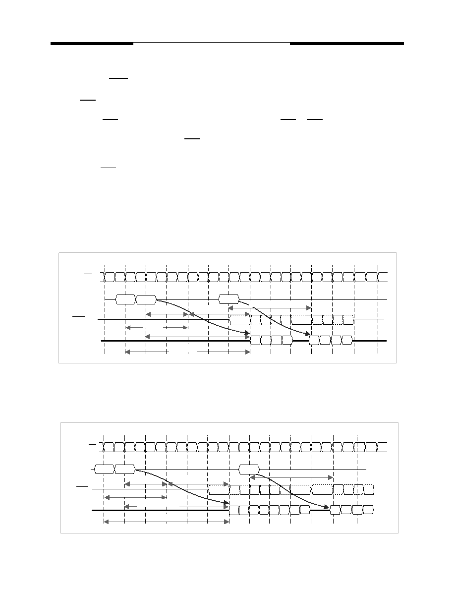
Read followed by a write to the same bank, Activate to Read delay < tRCDmin:
AL = 2 and CL = 3, RL = (AL + CL) = 5, WL = (RL -1) = 4, BL = 4
Dout0 Dout1 Dout2Dout3
CMD
DQ
0
2
34
5
6
7
8
9
10
11
12
-1
1
tRCD
AL = 2
" tRAC"
RL = AL + CL = 5
CL = 3
WL = RL -1 = 4
Din0 Din1
Din2 Din3
PostCAS1
DQS,
DQS
Activate
Read
Write
Bank A
CK, CK
Read followed by a write to the same bank, Activate to Read delay < tRCDmin:
AL = 2 and CL = 3, RL = (AL + CL) = 5, WL = (RL -1) = 4, BL = 8
CMD
DQ
0
2
34
5
6
7
8
9
10
11
12
1
tRCD
AL = 2
" tRAC"
RL = AL + CL = 5
CL = 3
WL = RL -1 = 4
PostCAS3
DQS,
DQS
Activate
Read
Bank A
Din0 Din1
Din2 Din3
Write
Bank A
Dout0
Dout1
Dout2 Dout3
Dout0
Dout1
Dout2 Dout3
CK, CK
相关PDF资料 |
PDF描述 |
|---|---|
| V59C1G01408QAUP25A | 256M X 4 DDR DRAM, PBGA68 |
| V59C1512164QALJ25AH | 32M X 16 DDR DRAM, PBGA92 |
| V59C1512164QALP37I | 32M X 16 DDR DRAM, PBGA92 |
| V59C1512164QAUJ5I | 32M X 16 DDR DRAM, PBGA92 |
| V59C1512164QAUP19AH | 32M X 16 DDR DRAM, PBGA92 |
相关代理商/技术参数 |
参数描述 |
|---|---|
| V5A010CB | 制造商:Honeywell Sensing and Control 功能描述:MICROSWITCH V5 PIN PLUNGER |
| V5A010CB | 制造商:Honeywell Sensing and Control 功能描述:MICROSWITCH V5 PIN PLUNGER |
| V5A010CB4D | 制造商:Honeywell Sensing and Control 功能描述:MICROSWITCH V5 ROLLER LEVER |
| V5A010CB4D | 制造商:Honeywell Sensing and Control 功能描述:MICROSWITCH V5 ROLLER LEVER |
| V5A010CB4E | 制造商:Honeywell Sensing and Control 功能描述:MICROSWITCH V5 ROLLER LEVER |
发布紧急采购,3分钟左右您将得到回复。