- 您现在的位置:买卖IC网 > PDF目录359401 > VN2450 (ELAN Microelctronics Corp .) N-Channel Enhancement-Mode Vertical DMOS FET(击穿电压500V,13Ω,N沟道增强型垂直DMOS结构场效应管) PDF资料下载
参数资料
| 型号: | VN2450 |
| 厂商: | ELAN Microelctronics Corp . |
| 英文描述: | N-Channel Enhancement-Mode Vertical DMOS FET(击穿电压500V,13Ω,N沟道增强型垂直DMOS结构场效应管) |
| 中文描述: | N沟道增强型场效应管垂直的DMOS(击穿电压的500V,13Ω,?沟道增强型垂直的DMOS结构场效应管) |
| 文件页数: | 1/4页 |
| 文件大小: | 28K |
| 代理商: | VN2450 |
1
VN2450
01/05/00
Supertex Inc. does not recommend the use of its products in life support applications and will not knowingly sell its products for use in such applications unless it receives an adequate "products liability
indemnification insurance agreement." Supertex does not assume responsibility for use of devices described and limits its liability to the replacement of devices determined to be defective due to
workmanship. No responsibility is assumed for possible omissions or inaccuracies. Circuitry and specifications are subject to change without notice. For complete liability information covering this and
other Supertex products, refer to the Supertex 1998 Databook.
VN2450
New Product
Advanced DMOS Technology
These low threshold enhancement-mode (normally-off) transis-
tors utilize a vertical DMOS structure and Supertex’s well-proven
silicon-gate manufacturing process. This combination produces
devices with the power handling capabilities of bipolar transistors
and with the high input impedance and positive temperature
coefficient inherent in MOS devices. Characteristic of all MOS
structures, these devices are free from thermal runaway and
thermally-induced secondary breakdown.
Supertex’s vertical DMOS FETs are ideally suited to a wide range
of switching and amplifying applications where high breakdown
voltage, high input impedance, low input capacitance, and fast
switching speeds are desired.
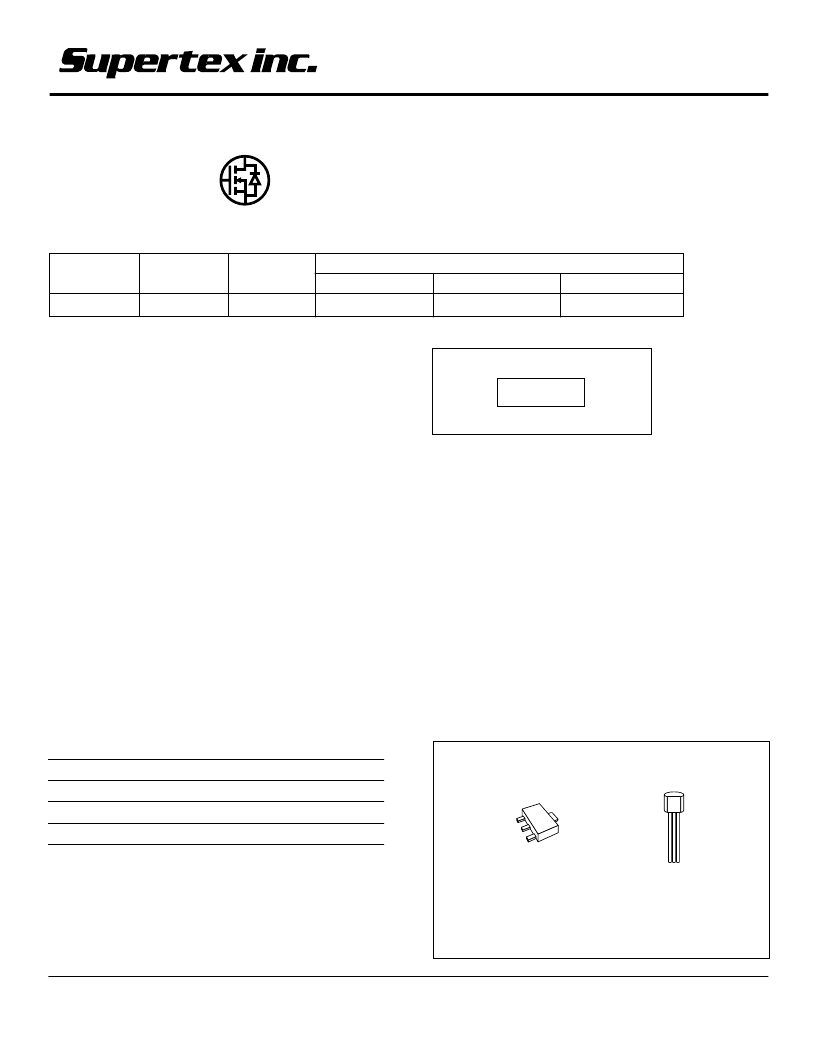
Package Options
Note: See Package Outline section for dimensions.
N-Channel Enhancement-Mode
Vertical DMOS FETs
Features
I
I
Free from secondary breakdown
I
I
Low input and output leakage
I
I
Low C
ISS
and fast switching speeds
High input impedance and high gain
I
I
Applications
I
I
Motor controls
I
I
Converters
I
I
Amplifiers
I
I
Switches
I
I
Power supply circuits
I
I
Drivers (relays, hammers, solenoids, lamps,
memories, displays, bipolar transistors, etc.)
BV
DSS
/
BV
DGS
500V
R
DS(ON)
(max)
I
D(ON)
(min)
TO-92
TO-243AA*
Die**
13
0.5A
VN2450N3
VN2450N8
VN2450MW
* Same as SOT-89 Product Supplied on 2000 piece carrier tape reels.
** Die in wafer form.
Ordering Information
Absolute Maximum Ratings
Drain-to-Source Voltage
BV
DSS
BV
DGS
±
20V
Drain-to-Gate Voltage
Gate-to-Source Voltage
Operating and Storage Temperature
-55
°
C to +150
°
C
Soldering Temperature*
*
Distance of 1.6 mm from case for 10 seconds.
300
°
C
TO-243AA
(SOT-89)
G
D
S
D
TO-92
S G D
Order Number / Package
Product marking for TO-243AA:
VN4E*
Where *= 2-week alpha date code
相关PDF资料 |
PDF描述 |
|---|---|
| VN2450 | N-Channel Enhancement-Mode Vertical DMOS FETs |
| VN2450N3 | N-Channel Enhancement-Mode Vertical DMOS FETs |
| VN2450N8 | N-Channel Enhancement-Mode Vertical DMOS FETs |
| VN2450NW | N-Channel Enhancement-Mode Vertical DMOS FETs |
| VN2460N3 | N-Channel Enhancement-Mode Vertical DMOS FETs |
相关代理商/技术参数 |
参数描述 |
|---|---|
| VN2450N3 | 功能描述:MOSFET 500V 13Ohm RoHS:否 制造商:STMicroelectronics 晶体管极性:N-Channel 汲极/源极击穿电压:650 V 闸/源击穿电压:25 V 漏极连续电流:130 A 电阻汲极/源极 RDS(导通):0.014 Ohms 配置:Single 最大工作温度: 安装风格:Through Hole 封装 / 箱体:Max247 封装:Tube |
| VN2450N3-G | 功能描述:MOSFET 500V 13Ohm RoHS:否 制造商:STMicroelectronics 晶体管极性:N-Channel 汲极/源极击穿电压:650 V 闸/源击穿电压:25 V 漏极连续电流:130 A 电阻汲极/源极 RDS(导通):0.014 Ohms 配置:Single 最大工作温度: 安装风格:Through Hole 封装 / 箱体:Max247 封装:Tube |
| VN2450N3-G P002 | 制造商:Supertex Inc 功能描述:N-CH Enhancmnt Mode MOSFET |
| VN2450N3-G P003 | 制造商:Supertex Inc 功能描述:N-CH Enhancmnt Mode MOSFET |
| VN2450N3-G P005 | 制造商:Supertex Inc 功能描述:N-CH Enhancmnt Mode MOSFET |
发布紧急采购,3分钟左右您将得到回复。