- 您现在的位置:买卖IC网 > PDF目录245689 > W3EG2256M72ASSR202AJD3SG (WHITE ELECTRONIC DESIGNS CORP) 512M X 72 DDR DRAM MODULE, 0.8 ns, DMA184 PDF资料下载
参数资料
| 型号: | W3EG2256M72ASSR202AJD3SG |
| 厂商: | WHITE ELECTRONIC DESIGNS CORP |
| 元件分类: | DRAM |
| 英文描述: | 512M X 72 DDR DRAM MODULE, 0.8 ns, DMA184 |
| 封装: | ROHS COMPLIANT, DIMM-184 |
| 文件页数: | 12/14页 |
| 文件大小: | 309K |
| 代理商: | W3EG2256M72ASSR202AJD3SG |
W3EG2256M72ASSR-JD3
-AJD3
-BJD3
7
White Electronic Designs
March, 2007
Rev. 4
White Electronic Designs Corporation (602) 437-1520 www.whiteedc.com
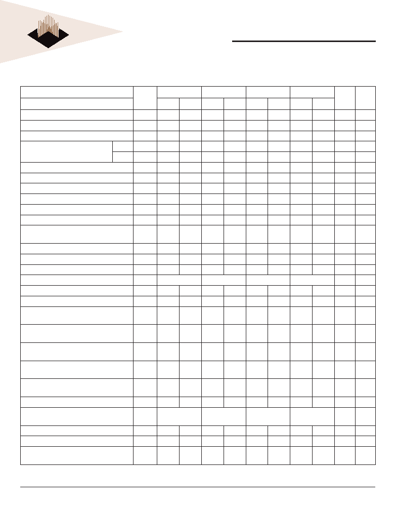
DDR SDRAM COMPONENT ELECTRICAL CHARACTERISTICS AND
RECOMMENDED AC OPERATING CONDITIONS
AC Characteristics
Symbol
335
262
263/265
202
Units
Notes
Parameter
Min
Max
Min
Max
Min
Max
Min
Max
Access window of DQs from CK, CK#
tAC
-0.7
+0.7
-0.7
+0.7
-0.75
+0.75
-0.8
+0.8
ns
CK high-level width
tCH
0.45
0.55
0.45
0.55
0.45
0.55
0.45
0.55
tCK
16
CK low-level width
tCL
0.45
0.55
0.45
0.55
0.45
0.55
0.45
0.55
tCK
16
Clock cycle time
CL=2.5 tCK (2.5)
6
12
7.5
12
7.5
12
8
12
ns
22
CL=2
tCK (2)
7.5
12
7.5
12
10
12
10
12
ns
22
DQ and DM input hold time relative to DQS
tDH
0.45
0.5
0.6
ns
14,17
DQ and DM input setup time relative to DQS
tDS
0.45
0.5
0.6
ns
14,17
DQ and DM input pulse width (for each input)
tDIPW
1.75
2
ns
17
Access window of DQS from CK, CK#
tDQSCK
-0.6
+0.60
-0.6
+0.60
-0.75
+0.75
-0.8
+0.8
ns
DQS input high pulse width
tDQSH
0.35
tCK
DQS input low pulse width
tDQSL
0.35
tCK
DQS-DQ skew, DQS to last DQ valid, per group,
per access
tDQSQ
0.45
0.5
ns
13,14
Write command to rst DQS latching transition
tDQSS
0.75
1.25
0.75
1.25
0.75
1.25
0.75
1.25
tCK
DQS falling edge to CK rising - setup time
tDSS
0.2
tCK
DQS falling edge from CK rising - hold time
tDSH
0.2
tCK
Half clock period
tHP
tCH(MIN), tCL(MIN)
ns
18
Data-out high-impedance window from CK, CK#
tHZ
-0.70
+0.70
-0.70
+0.70
-0.75
+0.75
-0.80
+0.80
ns
8,19
Data-out low-impedance window from CK, CK#
tLZ
-0.70
+0.70
-0.70
+0.70
-0.75
+0.75
-0.80
+0.80
ns
8,20
Address and control input hold time (fast slew
rate)
tIHf
0.75
0.90
1.1
ns
6
Address and control input set-up time (fast slew
rate)
tISf
0.75
0.90
1.1
ns
6
Address and control input hold time (slow slew
rate)
tIHs
0.80
1
1.1
ns
6
Address and control input setup time (slow slew
rate)
tISs
0.80
1
1.1
ns
6
Address and control input pulse width (for each
input)
tIPW
2.2
ns
LOAD MODE REGISTER command cycle time
tMRD
12
15
16
ns
DQ-DQS hold, DQS to rst DQ to go non-valid,
per access
tQH
tHP-tQHS
ns
13,14
Data hold skew factor
tQHS
0.55
0.75
1
ns
ACTIVE to PRECHARGE command
tRAS
45
70,000
45
70,000
45
70,000
45
70,000
ns
15
ACTIVE to READ with Auto precharge
command
tRAP
18
15
20
ns
Note: These parameters serve to support
SAMSUNG components based modules
相关PDF资料 |
PDF描述 |
|---|---|
| WED3DG644V75D1-S | 4M X 64 SYNCHRONOUS DRAM MODULE, ZMA144 |
| WF128K32N-120H1M | 512K X 8 FLASH 12V PROM MODULE, 120 ns, CHIP66 |
| WS1M32-35G4DI | 4M X 8 MULTI DEVICE SRAM MODULE, 35 ns, QMA68 |
| WPS512K32-35MZC | 512K X 32 MULTI DEVICE SRAM MODULE, 35 ns, ZMA72 |
| WMF2M8-150FLI5 | 2M X 8 FLASH 5V PROM, 150 ns, CDFP44 |
相关代理商/技术参数 |
参数描述 |
|---|---|
| W3EG2256M72ASSR202AJD3XG | 制造商:WEDC 制造商全称:White Electronic Designs Corporation 功能描述:4GB - 2x256Mx72 DDR SDRAM REGISTERED ECC, w/PLL |
| W3EG2256M72ASSR202JD3XG | 制造商:WEDC 制造商全称:White Electronic Designs Corporation 功能描述:4GB - 2x256Mx72 DDR SDRAM REGISTERED ECC, w/PLL |
| W3EG2256M72ASSR262AJD3XG | 制造商:WEDC 制造商全称:White Electronic Designs Corporation 功能描述:4GB - 2x256Mx72 DDR SDRAM REGISTERED ECC, w/PLL |
| W3EG2256M72ASSR262JD3XG | 制造商:WEDC 制造商全称:White Electronic Designs Corporation 功能描述:4GB - 2x256Mx72 DDR SDRAM REGISTERED ECC, w/PLL |
| W3EG2256M72ASSR263AJD3XG | 制造商:WEDC 制造商全称:White Electronic Designs Corporation 功能描述:4GB - 2x256Mx72 DDR SDRAM REGISTERED ECC, w/PLL |
发布紧急采购,3分钟左右您将得到回复。