- 您现在的位置:买卖IC网 > PDF目录376438 > X3N190-91 (CALOGIC LLC) 30V N-Channel PowerTrench MOSFET PDF资料下载
参数资料
| 型号: | X3N190-91 |
| 厂商: | CALOGIC LLC |
| 元件分类: | MOSFETs |
| 英文描述: | 30V N-Channel PowerTrench MOSFET |
| 中文描述: | 30V的N沟道的PowerTrench MOSFET的 |
| 文件页数: | 1/2页 |
| 文件大小: | 27K |
| 代理商: | X3N190-91 |
Dual P-Channel
Enhancement Mode MOSFET
General Purpose Ampifier
3N190 /3N191
FEATURES
Very High Input Impedance
High Gate Breakdown 3N190-3N191
Low Capacitance
ABSOLUTE MAXIMUM RATINGS
(T
A
= 25
o
C unless otherwise specified)
Drain-Source or Drain-Gate Voltage (Note 1)
3N190, 3N191 . . . . . . . . . . . . . . . . . . . . . . . . . . . . . . . . 40V
Transient Gate-Source Voltage (Note 1 and 2). . . . . . .
±
125V
Gate-Gate Voltage. . . . . . . . . . . . . . . . . . . . . . . . . . . . . .
±
80V
Drain Current (Note 1). . . . . . . . . . . . . . . . . . . . . . . . . . 50mA
Storage Temperature. . . . . . . . . . . . . . . . . . . -65
o
C to +200
o
C
Operating Temperature . . . . . . . . . . . . . . . . . -55
o
C to +150
o
C
Lead Temperature (Soldering, 10sec). . . . . . . . . . . . . +300
o
C
Power Dissipation
One Side . . . . . . . . . . . . . . . . . . . . . . . . . . . . . . . . . 300mW
Both Sides . . . . . . . . . . . . . . . . . . . . . . . . . . . . . . . . 525mW
Total Derating above 25
o
C. . . . . . . . . . . . . . . . . . 4.2mW/
o
C
NOTE:
Stresses above those listed under "Absolute Maximum
Ratings" may cause permanent damage to the device. These are
stress ratings only and functional operation of the device at these or
any other conditions above those indicated in the operational sections
of the specifications is not implied. Exposure to absolute maximum
rating conditions for extended periods may affect device reliability.
ORDERING INFORMATION
Part
3N190-91
X3N190-91 Sorted Chips in Carriers
Package
Hermetic TO-99
Temperature Range
-55
o
C to +150
o
C
-55
o
C to +150
o
C
C ORPORATION
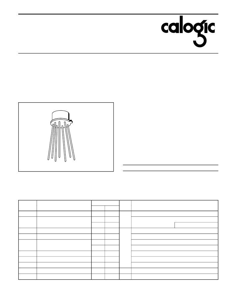
PIN CONFIGURATION
S2
G1
D2
D1
G2
S1
C
TO-99
2506
ELECTRICAL CHARACTERISTICS
(T
A
= 25
o
C and V
BS
= 0 unless otherwise specified)
SYMBOL
PARAMETER
3N190/91
UNITS
TEST CONDITIONS
MIN
MAX
I
GSSR
Gate Reverse Current
10
pA
V
GS
= 40V
I
GSSF
Gate Forward Current
-10
V
GS
= -40V
-25
T
A
= +125
o
C
BV
DSS
Drain-Source Breakdown Voltage
-40
V
I
D
= -10
μ
A
BV
SDS
Source-Drain Breakdown Voltage
-40
I
S
= -10
μ
A, V
BD
= 0
V
GS(th)
Threshold Voltage
-2.0
-5.0
V
DS
= -15V, I
D
= -10
μ
A
-2.0
-5.0
V
DS
= V
GS
, I
D
= -10
μ
A
V
GS
Gate Source Voltage
-3.0
-6.5
V
DS
= -15V, I
D
= -500
μ
A
I
DSS
Zero Gate Voltage Drain Current
-200
V
DS
= -15V
I
SDS
Source Drain Current
-400
V
SD
= -15V, V
DB
= 0
r
DS(on)
Drain-Source on Resistance
300
ohms
V
DS
= -20V, I
D
= -100
μ
A
I
D(on)
On Drain Current
-5.0
-30.0
mA
V
DS
= -15V, V
GS
= -10V
相关PDF资料 |
PDF描述 |
|---|---|
| X40020S14IZ-A | Dual Voltage Monitor with Intergrated CPU Supervisor |
| X40020S14IZ-B | Dual Voltage Monitor with Intergrated CPU Supervisor |
| X40020S14Z-A | Dual Voltage Monitor with Intergrated CPU Supervisor |
| X40020S14Z-B | Dual Voltage Monitor with Intergrated CPU Supervisor |
| X40020V14IZ-A | Dual Voltage Monitor with Intergrated CPU Supervisor |
相关代理商/技术参数 |
参数描述 |
|---|---|
| X3P3E-RD | 制造商:3M Electronic Products Division 功能描述:X3 Ear Defender Helmet Mounted 32dB |
| X3PM-001MPG | 制造商:FUJIKURA 制造商全称:FUJIKURA 功能描述:Pre-amplified/3V Excitation/Gauge |
| X3PM-001MPGR | 制造商:FUJIKURA 制造商全称:FUJIKURA 功能描述:Pre-amplified/3V Excitation/Gauge |
| X3PM-050KPG | 制造商:FUJIKURA 制造商全称:FUJIKURA 功能描述:Pre-amplified/3V Excitation/Gauge |
| X3PM-050KPGR | 制造商:FUJIKURA 制造商全称:FUJIKURA 功能描述:Pre-amplified/3V Excitation/Gauge |
发布紧急采购,3分钟左右您将得到回复。