- 您现在的位置:买卖IC网 > PDF目录24690 > 05F6971 IC-ELECTROMETER AMPLIFIER PDF资料下载
参数资料
| 型号: | 05F6971 |
| 英文描述: | IC-ELECTROMETER AMPLIFIER |
| 中文描述: | 集成电路静电计放大器 |
| 文件页数: | 2/12页 |
| 文件大小: | 347K |
| 代理商: | 05F6971 |
AD524
REV. C
–10–
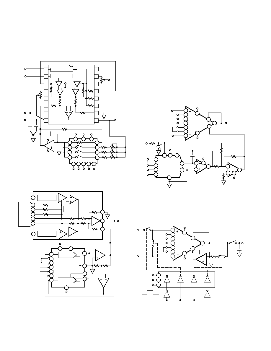
The AD524 can also be connected for gain in the output stage.
Figure 42 shows an AD547 used as an active attenuator in the
output amplifier’s feedback loop. The active attenuation pre-
sents a very low impedance to the feedback resistors therefore
minimizing the common rejection ratio degradation.
–IN
+IN
11
12
13
16
15
14
10
9
20k
+Vs
20k
AD524
R2
10k
20k
4.44k
404
40
PROTECTION
1F
35V
–Vs
16
1
3
4
5
6
7
8
PROTECTION
1
2
4
5
6
7
8
(+INPUT)
(–INPUT)
OUTPUT
OFFSET
NULL
+Vs
10pF
20k
AD711
–Vs
+Vs
9
15
14
2
10
AD7590
VSS
VDD GND
13
11
39.2k
28.7k
316k
VOUT
1k
1k
1k
TO
–V
3
10k
INPUT
OFFSET
NULL
12
VDD A2 A3 A4 WR
Figure 42. Programmable Output Gain
16
6
+Vs
WR
14
7
15
9
2
3
16
11
12
13
VOUT
1
18
19
PROTECTION
3
17
10
6
2
20
1
4
Vb
AD524
DAC A
DB0
256:1
1/2
AD712
20k
+INPUT
(–INPUT)
G = 10
–INPUT
(+INPUT)
G = 100
G = 1000
RG2
RG1
4.44k
404k
40k
PROTECTION
20k
20k
20k
20k
20k
DAC B
DB7
AD7528
5
DATA
INPUTS
CS
DAC A/DAC B
1/2
AD712
Figure 43. Programmable Output Gain Using a DAC
Another method for developing the switching scheme is to use a
DAC. The AD7528 dual DAC which acts essentially as a pair of
switched resistive attenuators having high analog linearity and
symmetrical bipolar transmission is ideal in this application. The
multiplying DAC’s advantage is that it can handle inputs of
either polarity or zero without affecting the programmed gain.
The circuit shown uses an AD7528 to set the gain (DAC A) and
to perform a fine adjustment (DAC B).
AUTO-ZERO CIRCUITS
In many applications it is necessary to provide very accurate
data in high gain configurations. At room temperature the offset
effects can be nulled by the use of offset trimpots. Over the op-
erating temperature range, however, offset nulling becomes a
problem. The circuit of Figure 44 show a CMOS DAC operat-
ing in the bipolar mode and connected to the reference terminal
to provide software controllable offset adjustments.
WR
CS
+INPUT
G = 10
–INPUT
G = 100
G = 1000
RG2
RG1
+Vs
16
14
15
6
7
4
2
3
AD7524
1
2
3
7
8
+Vs
–Vs
+Vs
4
11
12
13
2
16
13
12
11
3
1
9
10
6
8
OUT2
39k
AD589
MSB
LSB
DATA
INPUTS
–Vs
1
1/2
AD712
1/2
AD712
R3
20k
R4
10k
R6
5k
C1
GND
R5
20k
OUT1
VREF
AD524
5
Figure 44. Software Controllable Offset
In many applications complex software algorithms for auto-zero
applications are not available. For those applications Figure 45
provides a hardware solution.
RG2
RG1
+Vs
7
–Vs
2
16
13
12
11
3
1
9
8
AD524
15
16
14
13
VDD
GND
0.1F LOW
LEAKAGE
6
10
CH
1k
VOUT
910
2
1
8
A1
A2
A3
A4
200s
VSS
ZERO PULSE
AD7510KD
AD711
11
12
Figure 45. Auto-Zero Circuit
相关PDF资料 |
PDF描述 |
|---|---|
| 934045690118 | BUF OR INV BASED PRPHL DRVR |
| 934045770114 | S BAND, Si, NPN, RF POWER TRANSISTOR |
| 934045780114 | S BAND, Si, NPN, RF POWER TRANSISTOR |
| 934045790114 | S BAND, Si, NPN, RF POWER TRANSISTOR |
| 934045800114 | S BAND, Si, NPN, RF POWER TRANSISTOR |
相关代理商/技术参数 |
参数描述 |
|---|---|
| 05FD101J03 | 制造商: 功能描述: 制造商:undefined 功能描述: |
| 05FD111J03 | 制造商: 功能描述: 制造商:undefined 功能描述: |
| 05FD161J03 | 制造商: 功能描述: 制造商:undefined 功能描述: |
| 05FD241J03 | 制造商: 功能描述: 制造商:undefined 功能描述: |
| 05FD271J03 | 制造商: 功能描述: 制造商:undefined 功能描述: |
发布紧急采购,3分钟左右您将得到回复。