- 您现在的位置:买卖IC网 > PDF目录222090 > 1339-31DCGI8 (INTEGRATED DEVICE TECHNOLOGY INC) 1 TIMER(S), REAL TIME CLOCK, PDSO8 PDF资料下载
参数资料
| 型号: | 1339-31DCGI8 |
| 厂商: | INTEGRATED DEVICE TECHNOLOGY INC |
| 元件分类: | 时钟/数据恢复及定时提取 |
| 英文描述: | 1 TIMER(S), REAL TIME CLOCK, PDSO8 |
| 封装: | 0.150 INCH, ROHS COMPLIANT, SOIC-8 |
| 文件页数: | 4/26页 |
| 文件大小: | 330K |
| 代理商: | 1339-31DCGI8 |
IDT1339
REAL-TIME CLOCK WITH SERIAL I2C INTERFACE
RTC
IDT
REAL-TIME CLOCK WITH SERIAL I2C INTERFACE
12
IDT1339
REV N 060311
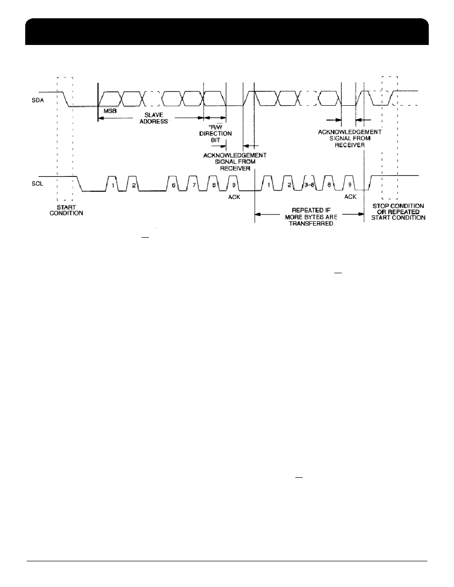
Data Transfer on I2C Serial Bus
Depending upon the state of the R/W bit, two types of data
transfer are possible:
1) Data transfer from a master transmitter to a slave
receiver. The first byte transmitted by the master is the
slave address. Next follows a number of data bytes. The
slave returns an acknowledge bit after each received byte.
Data is transferred with the most significant bit (MSB) first.
2) Data transfer from a slave transmitter to a master
receiver. The first byte (the slave address) is transmitted by
the master. The slave then returns an acknowledge bit. This
is followed by the slave transmitting a number of data bytes.
The master returns an acknowledge bit after all received
bytes other than the last byte. At the end of the last received
byte, a “not acknowledge” is returned. The master device
generates all of the serial clock pulses and the START and
STOP conditions. A transfer is ended with a STOP condition
or with a repeated START condition. Since a repeated
START condition is also the beginning of the next serial
transfer, the bus is not released. Data is transferred with the
most significant bit (MSB) first.
The IDT1339 can operate in the following two modes:
1) Slave Receiver Mode (Write Mode): Serial data and
clock are received through SDA and SCL. After each byte is
received an acknowledge bit is transmitted. START and
STOP conditions are recognized as the beginning and end
of a serial transfer. Address recognition is performed by
hardware after reception of the slave address and direction
bit (see the “Data Write–Slave Receiver Mode” figure). The
slave address byte is the first byte received after the START
condition is generated by the master. The slave address
byte contains the 7-bit IDT1339 address, which is 1101000,
followed by the direction bit (R/W), which is 0 for a write.
After receiving and decoding the slave address byte the
slave outputs an acknowledge on the SDA line. After the
IDT1339 acknowledges the slave address + write bit, the
master transmits a register address to the IDT1339. This
sets the register pointer on the IDT1339, with the IDT1339
acknowledging the transfer. The master may then transmit
zero or more bytes of data, with the IDT1339 acknowledging
each byte received. The address pointer increments after
each data byte is transferred. The master generates a STOP
condition to terminate the data write.
2) Slave Transmitter Mode (Read Mode): The first byte is
received and handled as in the slave receiver mode.
However, in this mode, the direction bit indicates that the
transfer direction is reversed. Serial data is transmitted on
SDA by the IDT1339 while the serial clock is input on SCL.
START and STOP conditions are recognized as the
beginning and end of a serial transfer (see the “Data
Read–Slave Transmitter Mode” figure). The slave address
byte is the first byte received after the START condition is
generated by the master. The slave address byte contains
the 7-bit IDT1339 address, which is 1101000, followed by
the direction bit (R/W), which is 1 for a read. After receiving
and decoding the slave address byte the slave outputs an
acknowledge on the SDA line. The IDT1339 then begins to
transmit data starting with the register address pointed to by
相关PDF资料 |
PDF描述 |
|---|---|
| 13715-806-XTD | 300 MHz, OTHER CLOCK GENERATOR, PDSO16 |
| 1374610-3 | INTERCONNECTION DEVICE |
| 1376137-1 | POWER CONNECTOR |
| 1380B-8 | BRASS, GOLD FINISH, PCB TERMINAL |
| 1390D-17 | BRASS, PCB TERMINAL |
相关代理商/技术参数 |
参数描述 |
|---|---|
| 1339-31DVGI | 功能描述:实时时钟 实时时钟 RoHS:否 制造商:Microchip Technology 功能:Clock, Calendar. Alarm RTC 总线接口:I2C 日期格式:DW:DM:M:Y 时间格式:HH:MM:SS RTC 存储容量:64 B 电源电压-最大:5.5 V 电源电压-最小:1.8 V 最大工作温度:+ 85 C 最小工作温度: 安装风格:Through Hole 封装 / 箱体:PDIP-8 封装:Tube |
| 1339-31DVGI8 | 功能描述:实时时钟 实时时钟 RoHS:否 制造商:Microchip Technology 功能:Clock, Calendar. Alarm RTC 总线接口:I2C 日期格式:DW:DM:M:Y 时间格式:HH:MM:SS RTC 存储容量:64 B 电源电压-最大:5.5 V 电源电压-最小:1.8 V 最大工作温度:+ 85 C 最小工作温度: 安装风格:Through Hole 封装 / 箱体:PDIP-8 封装:Tube |
| 133933 | 制造商:ERNI Electronics 功能描述:133933 / MODULAR JACK |
| 133934 | 制造商:ERNI Electronics 功能描述:Conn Telephone/Telecom F 8 POS 2.54mm Solder ST Thru-Hole 8 Terminal 1 Port Tray Cat 5 |
| 1339342-1 | 功能描述:集管和线壳 1 Pair Double Red Pivot Conn RoHS:否 产品种类:1.0MM Rectangular Connectors 产品类型:Headers - Pin Strip 系列:DF50 触点类型:Pin (Male) 节距:1 mm 位置/触点数量:16 排数:1 安装风格:SMD/SMT 安装角:Right 端接类型:Solder 外壳材料:Liquid Crystal Polymer (LCP) 触点材料:Brass 触点电镀:Gold 制造商:Hirose Connector |
发布紧急采购,3分钟左右您将得到回复。