- 您现在的位置:买卖IC网 > Datasheet目录38 > 1B22AN (Analog Devices Inc)IC VOLTAGE CONVERTER PROG DIP Datasheet资料下载
参数资料
| 型号: | 1B22AN |
| 厂商: | Analog Devices Inc |
| 文件页数: | 3/4页 |
| 文件大小: | 224K |
| 描述: | IC VOLTAGE CONVERTER PROG DIP |
| 产品变化通告: | Product Change Notice 06/Jul/2009 |
| 标准包装: | 1 |
| 类型: | 电压和电流控制器 |
| 全量程: | ±50ppm/°C |
| 线性: | ±0.02% |
| 安装类型: | 通孔 |
| 封装/外壳: | 38-DIP(0.800",20.32mm),12 引线 |
| 供应商设备封装: | 12-DIP |
| 包装: | 散装 |
1B22
REV. B
3
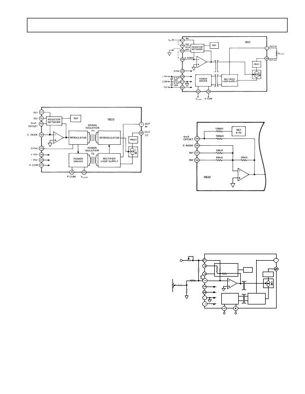
INSIDE THE 1B22
The 1B22 produces an isolated 4 to 20 mA or 0 to 20 mA out-
put current which is proportional to the input voltage and
independent of the output load resistance (Figure 1). The input
stage is configured as an inverting amplifier with a resistor net-
work to provide pin-strappable input ranges of 0 V to +5 V and
0 V to +10 V and output ranges of 0 to 20 mA and 4 to 20 mA.
The conditioned signal is modulated to generate a square wave
that drives transformer T1. The peak-to-peak amplitude of the
signal is proportional to V
IN
. An internal, high stability reference
with a nominal output voltage of +6.4 V is used to develop a
4 mA offset for the 4 to 20 mA current loop output.
Figure 1. 1B22 Functional Block Diagram
After passing through signal transformer T1, the amplitude
modulated signal is demodulated and filtered by a single pole
filter. This filtered output is the control signal for the voltage-
to-current converter stage. Timing information for the
demodulator is derived from the power transformer T2. The
1B22 outputs are protected from accidental shorts to ac line
voltages up to 240 V rms. Combined with 1500 V input to out-
put isolation, the 1B22 provides unbeatable protection against
transients, wiring errors and current loop short circuits to power
lines.
The dc-dc converter consists of a power driver, power trans-
former T2, a full wave rectifier and a filter. The dc-dc converter
provides the power for the output circuitry as well as the
isolated compliance voltage for the loop. This voltage is propor-
tional to V
LOOP
on the input side. The 1B22 requires ?5 V
supplies to power the input side circuitry and a +14 V to +30 V
supply for the dc-dc converter.
USING THE 1B22
Basic Interconnections: The 1B22 may be applied to achieve
rated performance as shown in Figure 2. For 0 V to 10 V signals
either IN1 or IN2 can be used for input; for 0 V to +5 V signals
jumper IN1 to IN2. Similarly, for 4 to 20 mA operation the
4 mA OFFSET node should be jumpered to the S. NODE,
while for 0 to 20 mA it should be tied to COM. Figure 3 shows
the functional diagram of the resistor network used in the 1B22.
For applications where a separate loop supply is not available,
the ?5 V supplies can be used by connecting +15 V to V
LOOP
(Pin 24) and COM to P.COM (Pin 25). For additional compli-
ance voltage, P.COM can be connected to 15 V to drive higher
loads.
Figure 2. Basic Interconnections
Figure 3. Internal Resistor Network
Optional Trim Adjustments: Figure 4 is an example of using
potentiometers for trimming gain and offset for a 0 V to +10 V
input and 4 to 20 mA output. The network for offset adjustment
keeps the resistors relatively small to minimize noise effects
while giving a sensitivity of ?% of span. The value of R1
should be 5 M& for the 0 V to +10 V range (for 0 V to +5 V
configurations, a 1.2 M& resistor should be used). For more
adjustment range, resistors smaller than 274 k& can be used.
IN2
4mA
OFF
50k
RESISTOR
NETWORK
REF
IN1
S. NODE
R1
POWER
DRIVER
RECTIFIER/
LOOP
SUPPLY
SYNC
+15V
COM
15V
V
LOOP
P. COM
PROT
OUT
HI
OUT
LO
20k
1k
V
IN
274k
50k
+15V
15V
1k
1B22
Figure 4. Optional Offset and Span Adjustment
相关PDF资料 |
PDF描述 |
|---|---|
| AD536AKQ | IC TRUE RMS/DC CONV 14CDIP |
| AD537SD | IC V/F CONV 14-CDIP |
| AD636JD | IC TRUE RMS/DC CONV MONO 14-CDIP |
| AD650SD | IC V-F/F-V CONV 1MHZ 14-CDIP |
| AD652SQ | IC V-F CONV SYNCH MONO 5V 16CDIP |
相关代理商/技术参数 |
参数描述 |
|---|---|
| 1B22AN | 制造商:Analog Devices 功能描述:SEMICONDUCTORSLINEAR 制造商:Analog Devices 功能描述:IC, VOLTAGE-TO-CURRENT CONVERTER, 12-DIP |
| 1B-23A-B | 制造商:FCI 功能描述: |
| 1B243 | 制造商:Ferraz Shawmut 功能描述: |
| 1B245 | 制造商:Ferraz Shawmut 功能描述: |
| 1B-24A | 制造商:FCI 功能描述:CONN CONT M/M 1 POS/1 POS ST - Tape and Reel |
发布紧急采购,3分钟左右您将得到回复。