参数资料
| 型号: | 1SMB28CAT3G |
| 厂商: | ON Semiconductor |
| 文件页数: | 5/7页 |
| 文件大小: | 0K |
| 描述: | TVS 600W 28V BIDIRECT SMB |
| 产品目录绘图: | SMB 600 Watt Top SMB 600 Watt Side 1 SMB 600 Watt Side 2 |
| 标准包装: | 1 |
| 电压 - 反向隔离(标准值): | 28V |
| 电压 - 击穿: | 31.1V |
| 功率(瓦特): | 600W |
| 电极标记: | 双向 |
| 安装类型: | 表面贴装 |
| 封装/外壳: | DO-214AA,SMB |
| 供应商设备封装: | SMB |
| 包装: | 标准包装 |
| 其它名称: | 1SMB28CAT3GOSDKR |
�� �
�
�1SMB10CAT3G� Series,� SZ1SMB10CAT3G� Series�
�APPLICATION� NOTES�
�Response� Time�
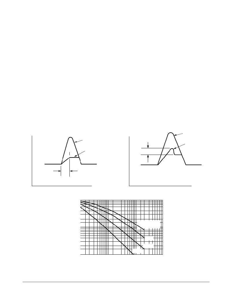
�In� most� applications,� the� transient� suppressor� device� is�
�placed� in� parallel� with� the� equipment� or� component� to� be�
�protected.� In� this� situation,� there� is� a� time� delay� associated�
�with� the� capacitance� of� the� device� and� an� overshoot�
�condition� associated� with� the� inductance� of� the� device� and�
�the� inductance� of� the� connection� method.� The� capacitive�
�effect� is� of� minor� importance� in� the� parallel� protection�
�scheme� because� it� only� produces� a� time� delay� in� the�
�transition� from� the� operating� voltage� to� the� clamp� voltage� as�
�shown� in� Figure� 5.�
�The� inductive� effects� in� the� device� are� due� to� actual�
�turn-on� time� (time� required� for� the� device� to� go� from� zero�
�current� to� full� current)� and� lead� inductance.� This� inductive�
�effect� produces� an� overshoot� in� the� voltage� across� the�
�equipment� or� component� being� protected� as� shown� in�
�Figure� 6.� Minimizing� this� overshoot� is� very� important� in� the�
�application,� since� the� main� purpose� for� adding� a� transient�
�suppressor� is� to� clamp� voltage� spikes.� The� SMB� series� have�
�a� very� good� response� time,� typically� <� 1� ns� and� negligible�
�inductance.� However,� external� inductive� effects� could�
�produce� unacceptable� overshoot.� Proper� circuit� layout,�
�minimum� lead� lengths� and� placing� the� suppressor� device� as�
�close� as� possible� to� the� equipment� or� components� to� be�
�protected� will� minimize� this� overshoot.�
�Some� input� impedance� represented� by� Z� in� is� essential� to�
�prevent� overstress� of� the� protection� device.� This� impedance�
�should� be� as� high� as� possible,� without� restricting� the� circuit�
�operation.�
�Duty� Cycle� Derating�
�The� data� of� Figure� 1� applies� for� non-repetitive� conditions�
�and� at� a� lead� temperature� of� 25� ?� C.� If� the� duty� cycle� increases,�
�the� peak� power� must� be� reduced� as� indicated� by� the� curves�
�of� Figure� 7.� Average� power� must� be� derated� as� the� lead� or�
�ambient� temperature� rises� above� 25� ?� C.� The� average� power�
�derating� curve� normally� given� on� data� sheets� may� be�
�normalized� and� used� for� this� purpose.�
�At� first� glance� the� derating� curves� of� Figure� 7� appear� to� be�
�in� error� as� the� 10� ms� pulse� has� a� higher� derating� factor� than�
�the� 10� m� s� pulse.� However,� when� the� derating� factor� for� a�
�given� pulse� of� Figure� 7� is� multiplied� by� the� peak� power� value�
�of� Figure� 1� for� the� same� pulse,� the� results� follow� the�
�expected� trend.�
�V�
�V� in� (TRANSIENT)�
�V�
�OVERSHOOT� DUE� TO�
�INDUCTIVE� EFFECTS�
�V� in� (TRANSIENT)�
�V� L�
�V� L�
�V� in�
�t� d�
�t� D� =� TIME� DELAY� DUE� TO� CAPACITIVE� EFFECT�
�Figure� 5.�
�1�
�0.7�
�0.5�
�0.3�
�0.2�
�0.1�
�0.07�
�0.05�
�0.03�
�0.02�
�t�
�Figure� 6.�
�PULSE� WIDTH�
�10� ms�
�1� ms�
�100� m� s�
�t�
�0.01�
�0.1� 0.2�
�0.5�
�1�
�10� m� s�
�2� 5� 10�
�20�
�50� 100�
�D,� DUTY� CYCLE� (%)�
�Figure� 7.� Typical� Derating� Factor� for� Duty� Cycle�
�http://onsemi.com�
�5�
�相关PDF资料 |
PDF描述 |
|---|---|
| 208457064001031 | CONNECTOR RECEPT 32POS STR |
| 108577048001025 | CONNECTOR HEADER 48POS STR |
| 208458096001028 | CONNECTOR RECEPT 96POS R/A |
| 108483006003049 | CONNECTOR HEADER 6POS R/A |
| 108483024001049 | CONNECTOR HEADER 24POS STR |
相关代理商/技术参数 |
参数描述 |
|---|---|
| 1SMB2EZ10 | 制造商:PANJIT 制造商全称:Pan Jit International Inc. 功能描述:GLASS PASSIVATED JUNCTION SILICON ZENER DIODES |
| 1SMB2EZ10_R1_00001 | 制造商:PanJit Touch Screens 功能描述: |
| 1SMB2EZ10_R2_00001 | 制造商:PanJit Touch Screens 功能描述: |
| 1SMB2EZ100 | 制造商:PANJIT 制造商全称:Pan Jit International Inc. 功能描述:GLASS PASSIVATED JUNCTION SILICON ZENER DIODES |
| 1SMB2EZ11 | 制造商:PANJIT 制造商全称:Pan Jit International Inc. 功能描述:GLASS PASSIVATED JUNCTION SILICON ZENER DIODES |
发布紧急采购,3分钟左右您将得到回复。