- 您现在的位置:买卖IC网 > PDF目录4238 > 24AA512T-I/ST14 (Microchip Technology)IC EEPROM 512KBIT 400KHZ 14TSSOP PDF资料下载
参数资料
| 型号: | 24AA512T-I/ST14 |
| 厂商: | Microchip Technology |
| 文件页数: | 9/36页 |
| 文件大小: | 0K |
| 描述: | IC EEPROM 512KBIT 400KHZ 14TSSOP |
| 产品培训模块: | I2C Serial EEPROM |
| 标准包装: | 2,500 |
| 格式 - 存储器: | EEPROMs - 串行 |
| 存储器类型: | EEPROM |
| 存储容量: | 512K (64K x 8) |
| 速度: | 100kHz,400kHz |
| 接口: | I²C,2 线串口 |
| 电源电压: | 1.7 V ~ 5.5 V |
| 工作温度: | -40°C ~ 85°C |
| 封装/外壳: | 14-TSSOP(0.173",4.40mm 宽) |
| 供应商设备封装: | 14-TSSOP |
| 包装: | 带卷 (TR) |
第1页第2页第3页第4页第5页第6页第7页第8页当前第9页第10页第11页第12页第13页第14页第15页第16页第17页第18页第19页第20页第21页第22页第23页第24页第25页第26页第27页第28页第29页第30页第31页第32页第33页第34页第35页第36页
�� �
�
�24AA512/24LC512/24FC512�
�5.0�
�DEVICE� ADDRESSING�
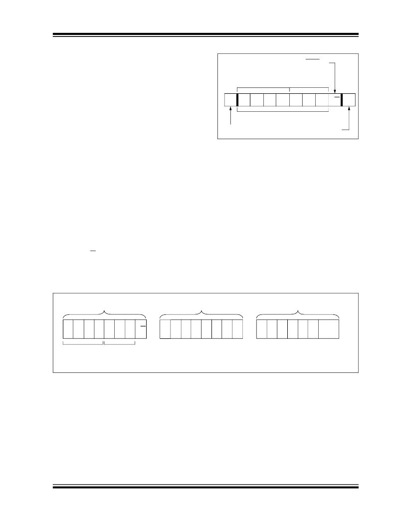
�FIGURE� 5-1:�
�CONTROL� BYTE� FORMAT�
�A� control� byte� is� the� first� byte� received� following� the�
�Start� condition� from� the� master� device� (Figure� 5-1).�
�Read/Write� Bit�
�The� control� byte� consists� of� a� 4-bit� control� code;� for� the�
�24XX512� this� is� set� as� ‘� 1010� ’� binary� for� read� and� write�
�operations.� The� next� three� bits� of� the� control� byte� are�
�Control� Code�
�Chip� Select�
�Bits�
�the� Chip� Select� bits� (A2,� A1� and� A0).� The� Chip� Select�
�bits� allow� the� use� of� up� to� eight� 24XX512� devices� on�
�S�
�1�
�0�
�1�
�0�
�A2�
�A1�
�A0� R/W� ACK�
�the� same� bus� and� are� used� to� select� which� device� is�
�accessed.� The� Chip� Select� bits� in� the� control� byte� must�
�Slave� Address�
�correspond� to� the� logic� levels� on� the� corresponding� A2,�
�A1� and� A0� pins� for� the� device� to� respond.� These� bits�
�are� in� effect� the� three� Most� Significant� bits� of� the� word�
�address.�
�Start� Bit�
�5.1�
�Acknowledge� Bit�
�Contiguous� Addressing� Across�
�The� last� bit� of� the� control� byte� defines� the� operation� to�
�be� performed.� When� set� to� a� one� a� read� operation� is�
�selected� and� when� set� to� a� zero� a� write� operation� is�
�selected.� The� next� two� bytes� received� define� the�
�address� of� the� first� data� byte� (Figure� 5-2).� Because� all�
�A15…A0� are� used,� there� are� no� upper� address� bits� that�
�are� “don’t� care”.� The� upper� address� bits� are� transferred�
�first,� followed� by� the� Less� Significant� bits.�
�Following� the� Start� condition,� the� 24XX512� monitors�
�the� SDA� bus� checking� the� device� type� identifier� being�
�transmitted.� Upon� receiving� a� ‘� 1010� ’� code� and� appro-�
�priate� device� select� bits,� the� slave� device� outputs� an�
�Acknowledge� signal� on� the� SDA� line.� Depending� on� the�
�state� of� the� R/W� bit,� the� 24XX512� will� select� a� read� or�
�write� operation.�
�Multiple� Devices�
�The� Chip� Select� bits� A2,� A1� and� A0� can� be� used� to�
�expand� the� contiguous� address� space� for� up� to� 4� Mbit�
�by� adding� up� to� eight� 24XX512� devices� on� the� same�
�bus.� In� this� case,� software� can� use� A0� of� the� control�
�byte� as� address� bit� A16;� A1� as� address� bit� A17;� and� A2�
�as� address� bit� A18.� It� is� not� possible� to� sequentially�
�read� across� device� boundaries.�
�FIGURE� 5-2:�
�ADDRESS� SEQUENCE� BIT� ASSIGNMENTS�
�Control� Byte�
�Address� High� Byte�
�Address� Low� Byte�
�0� R/W�
�1�
�0�
�1�
�0�
�A�
�2�
�A�
�1�
�A�
�A� A� A� A� A� A�
�15� 14� 13� 12� 11� 10�
�A�
�9�
�A�
�8�
�A�
�7�
�?�
�?�
�?�
�?�
�?�
�?�
�A�
�0�
�Control�
�Code�
�Chip�
�Select�
�Bits�
�?� 2010� Microchip� Technology� Inc.�
�DS21754M-page� 9�
�相关PDF资料 |
PDF描述 |
|---|---|
| XC5VLX30-1FF324C | IC FPGA VIRTEX-5 30K 324FBGA |
| SST39LF040-45-4C-NHE-T | IC FLASH MPF 4MBIT 45NS 32-PLCC |
| SST39VF040-70-4C-B3KE | IC FLASH MPF 4MBIT 70NS 48TFBGA |
| XC4VLX15-11FF668I | IC FPGA VIRTEX-4LX 668FFBGA |
| XC4VLX15-11FFG668I | IC FPGA VIRTEX-4 LX 15K 668FCBGA |
相关代理商/技术参数 |
参数描述 |
|---|---|
| 24AA515-I/P | 功能描述:电可擦除可编程只读存储器 64kx8 64B - 1.8V RoHS:否 制造商:Atmel 存储容量:2 Kbit 组织:256 B x 8 数据保留:100 yr 最大时钟频率:1000 KHz 最大工作电流:6 uA 工作电源电压:1.7 V to 5.5 V 最大工作温度:+ 85 C 安装风格:SMD/SMT 封装 / 箱体:SOIC-8 |
| 24AA515-I/SM | 功能描述:电可擦除可编程只读存储器 64kx8 64B - 1.8V RoHS:否 制造商:Atmel 存储容量:2 Kbit 组织:256 B x 8 数据保留:100 yr 最大时钟频率:1000 KHz 最大工作电流:6 uA 工作电源电压:1.7 V to 5.5 V 最大工作温度:+ 85 C 安装风格:SMD/SMT 封装 / 箱体:SOIC-8 |
| 24AA515T-I/SM | 功能描述:电可擦除可编程只读存储器 64kx8 64B - 1.8V RoHS:否 制造商:Atmel 存储容量:2 Kbit 组织:256 B x 8 数据保留:100 yr 最大时钟频率:1000 KHz 最大工作电流:6 uA 工作电源电压:1.7 V to 5.5 V 最大工作温度:+ 85 C 安装风格:SMD/SMT 封装 / 箱体:SOIC-8 |
| 24AA52-I/MC | 功能描述:电可擦除可编程只读存储器 256x8 - 2.5V Industrial Temp RoHS:否 制造商:Atmel 存储容量:2 Kbit 组织:256 B x 8 数据保留:100 yr 最大时钟频率:1000 KHz 最大工作电流:6 uA 工作电源电压:1.7 V to 5.5 V 最大工作温度:+ 85 C 安装风格:SMD/SMT 封装 / 箱体:SOIC-8 |
| 24AA52-I/MCG | 功能描述:电可擦除可编程只读存储器 256x8 - 2.5V Industrial Temp RoHS:否 制造商:Atmel 存储容量:2 Kbit 组织:256 B x 8 数据保留:100 yr 最大时钟频率:1000 KHz 最大工作电流:6 uA 工作电源电压:1.7 V to 5.5 V 最大工作温度:+ 85 C 安装风格:SMD/SMT 封装 / 箱体:SOIC-8 |
发布紧急采购,3分钟左右您将得到回复。