参数资料
| 型号: | 24C65/SM |
| 厂商: | Microchip Technology |
| 文件页数: | 6/24页 |
| 文件大小: | 0K |
| 描述: | IC EEPROM 64KBIT 400KHZ 8SOIC |
| 产品培训模块: | I2C Serial EEPROM |
| 标准包装: | 90 |
| 格式 - 存储器: | EEPROMs - 串行 |
| 存储器类型: | EEPROM |
| 存储容量: | 64K (8K x 8) |
| 速度: | 400kHz |
| 接口: | I²C,2 线串口 |
| 电源电压: | 4.5 V ~ 6 V |
| 工作温度: | 0°C ~ 70°C |
| 封装/外壳: | 8-SOIC(0.209",5.30mm 宽) |
| 供应商设备封装: | 8-SOIJ |
| 包装: | 管件 |
| 产品目录页面: | 1447 (CN2011-ZH PDF) |
�� �
�
�24AA65/24LC65/24C65�
�3.6�
�Device� Addressing�
�4.0�
�WRITE� OPERATION�
�A� control� byte� is� the� first� byte� received� following� the�
�Start� condition� from� the� master� device.� The� control� byte�
�4.1�
�Byte� Write�
�consists� of� a� four-bit� control� code,� for� the� 24XX65� this�
�is� set� as� ‘� 1010� ’� binary� for� read� and� write� operations.�
�The� next� three� bits� of� the� control� byte� are� the� device�
�select� bits� (A2,� A1,� A0).� They� are� used� by� the� master�
�device� to� select� which� of� the� eight� devices� are� to� be�
�accessed.� These� bits� are� in� effect� the� three� Most�
�Significant� bits� of� the� word� address.� The� last� bit� of� the�
�control� byte� defines� the� operation� to� be� performed.�
�When� set� to� a� one� a� read� operation� is� selected,� when�
�set� to� a� zero� a� write� operation� is� selected.� The� next� two�
�bytes� received� define� the� address� of� the� first� data� byte�
�(Figure� 4-1).� Because� only� A12..A0� are� used,� the�
�upper� three� address� bits� must� be� zeros.� The� Most�
�Significant� bit� of� the� Most� Significant� Byte� is� transferred�
�first.� Following� the� Start� condition,� the� 24XX65�
�monitors� the� SDA� bus� checking� the� device� type�
�identifier� being� transmitted.� Upon� receiving� a� ‘� 1010� ’�
�code� and� appropriate� device� select� bits,� the� slave�
�device� (24XX65)� outputs� an� Acknowledge� signal� on� the�
�Following� the� Start� condition� from� the� master,� the� con-�
�trol� code� (four� bits),� the� device� select� (three� bits),� and�
�the� R/W� bit� which� is� a� logic� low,� is� placed� onto� the� bus�
�by� the� master� transmitter.� This� indicates� to� the�
�addressed� slave� receiver� (24XX65)� that� a� byte� with� a�
�word� address� will� follow� after� it� has� generated� an�
�Acknowledge� bit� during� the� ninth� clock� cycle.� There-�
�fore,� the� next� byte� transmitted� by� the� master� is� the�
�high-order� byte� of� the� word� address� and� will� be� written�
�into� the� Address� Pointer� of� the� 24XX65.� The� next� byte�
�is� the� Least� Significant� Address� Byte.� After� receiving�
�another� Acknowledge� signal� from� the� 24XX65,� the�
�master� device� will� transmit� the� data� word� to� be� written�
�into� the� addressed� memory� location.� The� 24XX65�
�acknowledges� again� and� the� master� generates� a� Stop�
�condition.� This� initiates� the� internal� write� cycle,� and�
�during� this� time� the� 24XX65� will� not� generate�
�Acknowledge� signals� (Figure� 4-1).�
�SDA� line.� Depending� upon� the� state� of� the� R/W� bit,� the�
�24XX65� will� select� a� read� or� write� operation.�
�4.2�
�Page� Write�
�Operation� Control� Code�
�Device� Select�
�R/W�
�The� write� control� byte,� word� address� and� the� first� data�
�byte� are� transmitted� to� the� 24XX65� in� the� same� way� as�
�Read�
�Write�
�1010�
�1010�
�Device� Address�
�Device� Address�
�1�
�0�
�in� a� byte� write.� But� instead� of� generating� a� Stop�
�condition,� the� master� transmits� up� to� eight� pages� of�
�eight� data� bytes� each� (64� bytes� total),� which� are�
�temporarily� stored� in� the� on-chip� page� cache� of� the�
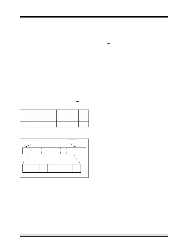
�FIGURE� 3-2:�
�START�
�CONTROL� BYTE�
�ALLOCATION�
�READ/WRITE�
�24XX65.� They� will� be� written� from� the� cache� into� the�
�EEPROM� array� after� the� master� has� transmitted� a� Stop�
�condition.� After� the� receipt� of� each� word,� the� six� lower�
�order� Address� Pointer� bits� are� internally� incremented� by�
�one.� The� higher� order� seven� bits� of� the� word� address�
�SLAVE� ADDRESS�
�R/W�
�A�
�remain� constant.� If� the� master� should� transmit� more�
�than� eight� bytes� prior� to� generating� the� Stop� condition�
�(writing� across� a� page� boundary),� the� address� counter�
�(lower� three� bits)� will� roll� over� and� the� pointer� will� be�
�incremented� to� point� to� the� next� line� in� the� cache.� This�
�1�
�0�
�1�
�0�
�A2�
�A1�
�A0�
�can� continue� to� occur� up� to� eight� times� or� until� the� cache�
�is� full,� at� which� time� a� Stop� condition� should� be�
�generated� by� the� master.� If� a� Stop� condition� is� not�
�received,� the� cache� pointer� will� roll� over� to� the� first� line�
�(byte� 0)� of� the� cache,� and� any� further� data� received� will�
�overwrite� previously� captured� data.� The� Stop� condition�
�can� be� sent� at� any� time� during� the� transfer.� As� with� the�
�byte� write� operation,� once� the� Stop� condition� is� received�
�an� internal� write� cycle� will� begin.� The� 64-byte� cache� will�
�continue� to� capture� data� until� a� Stop� condition� occurs� or�
�the� operation� is� aborted� (Figure� 4-2).�
�DS21073K-page� 6�
�?� 2008� Microchip� Technology� Inc.�
�相关PDF资料 |
PDF描述 |
|---|---|
| 24LC65-I/SM | IC EEPROM 64KBIT 400KHZ 8SOIC |
| SST39SF020A-70-4C-NHE | IC FLASH MPF 2MBIT 70NS 32PLCC |
| 24LC65/SM | IC EEPROM 64KBIT 400KHZ 8SOIC |
| 25AA256-I/MF | IC EEPROM 256KBIT 10MHZ 8DFN |
| 24FC512-I/SM | IC EEPROM 512KBIT 1MHZ 8SOIC |
相关代理商/技术参数 |
参数描述 |
|---|---|
| 24C65T/P | 制造商:未知厂家 制造商全称:未知厂家 功能描述:EEPROM |
| 24C65T-/P | 制造商:MICROCHIP 制造商全称:Microchip Technology 功能描述:64K 1.8V I2C Smart Serial O EEPROM |
| 24C65T/SM | 功能描述:电可擦除可编程只读存储器 8kx8 Smart RoHS:否 制造商:Atmel 存储容量:2 Kbit 组织:256 B x 8 数据保留:100 yr 最大时钟频率:1000 KHz 最大工作电流:6 uA 工作电源电压:1.7 V to 5.5 V 最大工作温度:+ 85 C 安装风格:SMD/SMT 封装 / 箱体:SOIC-8 |
| 24C65T-/SM | 制造商:MICROCHIP 制造商全称:Microchip Technology 功能描述:64K 1.8V I2C Smart Serial O EEPROM |
| 24C65T/SM | 制造商:Microchip Technology Inc 功能描述:EEPROM T&R 64K SMD 24C65 SOIC8 |
发布紧急采购,3分钟左右您将得到回复。