- 您现在的位置:买卖IC网 > PDF目录4323 > 24LC014T-I/ST (Microchip Technology)IC EEPROM 1KBIT 400KHZ 8TSSOP PDF资料下载
参数资料
| 型号: | 24LC014T-I/ST |
| 厂商: | Microchip Technology |
| 文件页数: | 5/36页 |
| 文件大小: | 0K |
| 描述: | IC EEPROM 1KBIT 400KHZ 8TSSOP |
| 产品培训模块: | I2C Serial EEPROM |
| 标准包装: | 2,500 |
| 格式 - 存储器: | EEPROMs - 串行 |
| 存储器类型: | EEPROM |
| 存储容量: | 1K (128 x 8) |
| 速度: | 400kHz |
| 接口: | I²C,2 线串口 |
| 电源电压: | 2.5 V ~ 5.5 V |
| 工作温度: | -40°C ~ 85°C |
| 封装/外壳: | 8-TSSOP(0.173",4.40mm 宽) |
| 供应商设备封装: | 8-TSSOP |
| 包装: | 带卷 (TR) |
| 其它名称: | 24LC014TI/ST |
第1页第2页第3页第4页当前第5页第6页第7页第8页第9页第10页第11页第12页第13页第14页第15页第16页第17页第18页第19页第20页第21页第22页第23页第24页第25页第26页第27页第28页第29页第30页第31页第32页第33页第34页第35页第36页
�� �
�
�24AA014/24LC014�
�2.0�
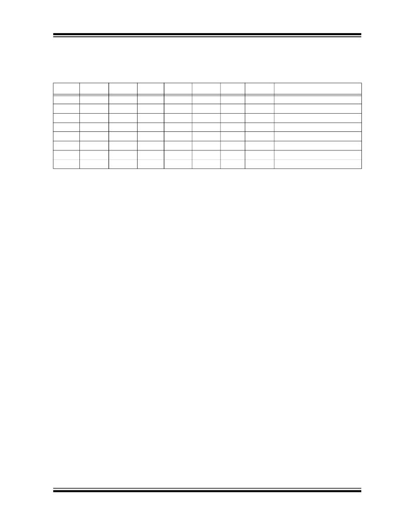
�PIN� DESCRIPTIONS�
�The� descriptions� of� the� pins� are� listed� in� Table� 2-1� .�
�TABLE� 2-1:�
�PIN� FUNCTION� TABLE�
�Name�
�A0�
�A1�
�A2�
�V� SS�
�SDA�
�SCL�
�WP�
�V� CC�
�PDIP�
�1�
�2�
�3�
�4�
�5�
�6�
�7�
�8�
�SOIC�
�1�
�2�
�3�
�4�
�5�
�6�
�7�
�8�
�TSSOP�
�1�
�2�
�3�
�4�
�5�
�6�
�7�
�8�
�DFN� (1)�
�1�
�2�
�3�
�4�
�5�
�6�
�7�
�8�
�TDFN� (1)�
�1�
�2�
�3�
�4�
�5�
�6�
�7�
�8�
�MSOP�
�1�
�2�
�3�
�4�
�5�
�6�
�7�
�8�
�SOT-23�
�5�
�4�
�—�
�2�
�3�
�1�
�—�
�6�
�Description�
�Chip� Address� Input�
�Chip� Address� Input�
�Chip� Address� Input�
�Ground�
�Serial� Address/Data� I/O�
�Serial� Clock�
�Write-Protect� Input�
�+1.7V� to� 5.5V� Power� Supply�
�Note� 1:� The� exposed� pad� on� the� DFN/TDFN� packages� can� be� connected� to� V� SS� or� left� floating.�
�2.1�
�A0,� A1,� A2� Chip� Address� Inputs�
�2.3�
�Serial� Clock� (SCL)�
�The� A0,� A1� and� A2� inputs� are� used� by� the� 24AA014/�
�24LC014� for� multiple� device� operation.� The� levels� on�
�these� inputs� are� compared� with� the� corresponding� bits�
�in� the� slave� address.� The� chip� is� selected� if� the� com-�
�pare� is� true.�
�Up� to� eight� devices� may� be� connected� to� the� same� bus�
�by� using� different� Chip� Select� bit� combinations.� These�
�inputs� must� be� connected� to� either� V� CC� or� V� SS� .�
�For� the� SOT-23� devices� up� to� four� devices� may� be� con-�
�The� SCL� input� is� used� to� synchronize� the� data� transfer�
�from� and� to� the� device.�
�2.4� Write-Protect� (WP)�
�This� pin� must� be� connected� to� either� V� SS� or� V� CC� .� If� tied�
�to� V� SS� ,� write� operations� are� enabled.� If� tied� to� V� CC� ,�
�write� operations� are� inhibited� but� read� operations� are�
�not� affected.�
�nected� to� the� same� bus� using� different� Chip� Select� bit�
�combinations.�
�3.0�
�FUNCTIONAL� DESCRIPTION�
�In� most� applications,� the� chip� address� inputs� A0,� A1�
�and� A2� are� hard-wired� to� logic� ‘� 0� ’� or� logic� ‘� 1� ’.� For�
�applications� in� which� these� pins� are� controlled� by� a�
�microcontroller� or� other� programmable� device,� the� chip�
�address� pins� must� be� driven� to� logic� ‘� 0� ’� or� logic� ‘� 1� ’�
�before� normal� device� operation� can� proceed.�
�The� 24AA014/24LC014� supports� a� bidirectional,� 2-wire�
�bus� and� data� transmission� protocol.� A� device� that�
�sends� data� onto� the� bus� is� defined� as� transmitter,� while�
�a� device� receiving� data� is� defined� as� a� receiver.� The�
�bus� has� to� be� controlled� by� a� master� device� which� gen-�
�erates� the� Serial� Clock� (SCL),� controls� the� bus� access�
�and� generates� the� Start� and� Stop� conditions,� while� the�
�2.2�
�Serial� Data� (SDA)�
�24AA014/24LC014� works� as� slave.� Both� master� and�
�slave� can� operate� as� transmitter� or� receiver,� but� the�
�SDA� is� a� bidirectional� pin� used� to� transfer� addresses�
�and� data� into� and� out� of� the� device.� Since� it� is� an� open-�
�drain� terminal,� the� SDA� bus� requires� a� pull-up� resistor�
�to� V� CC� (typical� 10� k� ?� for� 100� kHz,� 2� k� ??� for� 400� kHz).�
�For� normal� data� transfer,� SDA� is� allowed� to� change�
�only� during� SCL� low.� Changes� during� SCL� high� are�
�reserved� for� indicating� the� Start� and� Stop� conditions.�
�?� 2010� Microchip� Technology� Inc.�
�master� device� determines� which� mode� is� activated.�
�DS21809G-page� 5�
�相关PDF资料 |
PDF描述 |
|---|---|
| EP4SE230F29C3N | IC STRATIX IV E 230K 780FBGA |
| EP4SE230F29I4N | IC STRATIX IV FPGA 230K 780FBGA |
| EP4SGX290FF35C4N | IC STRATIX IV FPGA 290K 1152FBGA |
| EP4SGX180HF35I4 | IC STRATIX IV FPGA 180K 1152FBGA |
| EP4SGX180HF35C3 | IC STRATIX IV FPGA 180K 1152FBGA |
相关代理商/技术参数 |
参数描述 |
|---|---|
| 24LC01B | 制造商:MICROCHIP 制造商全称:Microchip Technology 功能描述:1K I2C? Serial EEPROM |
| 24LC01B/MS | 制造商:未知厂家 制造商全称:未知厂家 功能描述:EEPROM |
| 24LC01B/MT | 制造商:未知厂家 制造商全称:未知厂家 功能描述:I2C Serial EEPROM |
| 24LC01B-/OT | 制造商:未知厂家 制造商全称:未知厂家 功能描述:I2C Serial EEPROM |
| 24LC01B/P | 功能描述:电可擦除可编程只读存储器 128x8 - 1.8V RoHS:否 制造商:Atmel 存储容量:2 Kbit 组织:256 B x 8 数据保留:100 yr 最大时钟频率:1000 KHz 最大工作电流:6 uA 工作电源电压:1.7 V to 5.5 V 最大工作温度:+ 85 C 安装风格:SMD/SMT 封装 / 箱体:SOIC-8 |
发布紧急采购,3分钟左右您将得到回复。